Prices for established semiconductor processes are rising, while major foundries are shifting capacity. This is relevant for developers in industrial electronics, the automotive sector, medical technology, and measurement technology. At the same time, specialty foundries are investing in precisely these technologies. So what’s behind this trend?
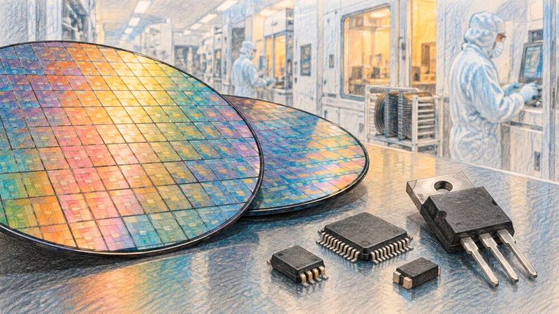
Established semiconductor processes: While some foundries are reducing their manufacturing capacity, others are making targeted investments in specialized technologies. For developers in industrial electronics, the automotive industry, and medical technology, the long-term availability and cost of components are crucial.
(Image: Dall-E / AI-generated)
In semiconductor manufacturing, much of the focus revolves around ever-smaller feature sizes. At least, that’s the impression one might get when attention is once again centered on the latest manufacturing nodes. For much of the electronics industry, the latest manufacturing technology and processes may briefly pique interest, but the reality of day-to-day operations looks quite different.
Rather, there is a demand for semiconductors that operate reliably, meet specific electrical requirements, and remain available for many years. Whether they are manufactured using a 180-nm or a 28-nm process is not necessarily a matter of technological progress.
Accordingly, current developments in so-called “mature nodes”—that is, established semiconductor processes—are of great interest: While major foundries are reducing or reallocating parts of their manufacturing capacity, demand for certain technologies is growing. Market researchers at Trendforce are therefore observing rising manufacturing prices and expect this trend to continue through 2027.
For companies in German-speaking countries that develop and manufacture electronics, this raises a very practical question: What happens if the production of those semiconductors—on which numerous industrial products rely—also becomes more expensive?
200-mm (8-inch) Manufacturing: Prices Rise by Up to 15 Percent
Current foundry prices illustrate just how significantly market conditions are changing. According to data from Trendforce, prices for 200-mm manufacturing rose by an average of 5 to 15 percent from the first to the second quarter of 2026. The average utilization rate for 200-mm production at the ten largest foundries reached approximately 88 percent in 2026. Market researchers expect this figure to rise to 90 percent in the second half of the year. Earlier this year, Trendforce had also forecast a 2.4 percent global decline in 200-mm capacity for 2026.
A key driver is the shift in demand; after all, as is to be expected in these times, AI plays a major role in this. AI data centers require not only high-performance processors and memory, but also numerous components for power supply, voltage regulation, and power management. In particular, power management ICs (PMICs) and certain discrete power semiconductors continue to be manufactured on a large scale using 200-mm wafers.
At the same time, major contract manufacturers such as TSMC and Samsung according to Trendforce, are reducing parts of their 200-mm capacity or using existing production lines for other products. Other foundries are shifting resources toward higher-margin applications. Not surprisingly, this is increasing the pressure on the remaining capacity.
However, this trend is not limited to 200-mm wafers. Price pressure is also evident in established processes on 300-mm (12-inch) wafers, particularly for certain high-voltage technologies. For individual processes with limited capacity, price increases of five to ten percent were projected between the second and third quarters of 2026.
This does not necessarily mean that all established semiconductor processes will become scarce. Capacity utilization, demand, and price trends vary significantly depending on the manufacturing technology. The further price increases for 2027 described by further price increases for 2027 described by Trendforce are, as of now, merely forecasts or the subject of negotiations—not surcharges that have already been implemented across the board.
Date: 08.12.2025
Naturally, we always handle your personal data responsibly. Any personal data we receive from you is processed in accordance with applicable data protection legislation. For detailed information please see our privacy policy.
Consent to the use of data for promotional purposes
I hereby consent to Vogel Communications Group GmbH & Co. KG, Max-Planck-Str. 7-9, 97082 Würzburg including any affiliated companies according to §§ 15 et seq. AktG (hereafter: Vogel Communications Group) using my e-mail address to send editorial newsletters. A list of all affiliated companies can be found here
Newsletter content may include all products and services of any companies mentioned above, including for example specialist journals and books, events and fairs as well as event-related products and services, print and digital media offers and services such as additional (editorial) newsletters, raffles, lead campaigns, market research both online and offline, specialist webportals and e-learning offers. In case my personal telephone number has also been collected, it may be used for offers of aforementioned products, for services of the companies mentioned above, and market research purposes.
Additionally, my consent also includes the processing of my email address and telephone number for data matching for marketing purposes with select advertising partners such as LinkedIn, Google, and Meta. For this, Vogel Communications Group may transmit said data in hashed form to the advertising partners who then use said data to determine whether I am also a member of the mentioned advertising partner portals. Vogel Communications Group uses this feature for the purposes of re-targeting (up-selling, cross-selling, and customer loyalty), generating so-called look-alike audiences for acquisition of new customers, and as basis for exclusion for on-going advertising campaigns. Further information can be found in section “data matching for marketing purposes”.
In case I access protected data on Internet portals of Vogel Communications Group including any affiliated companies according to §§ 15 et seq. AktG, I need to provide further data in order to register for the access to such content. In return for this free access to editorial content, my data may be used in accordance with this consent for the purposes stated here. This does not apply to data matching for marketing purposes.
Right of revocation
I understand that I can revoke my consent at will. My revocation does not change the lawfulness of data processing that was conducted based on my consent leading up to my revocation. One option to declare my revocation is to use the contact form found at https://contact.vogel.de. In case I no longer wish to receive certain newsletters, I have subscribed to, I can also click on the unsubscribe link included at the end of a newsletter. Further information regarding my right of revocation and the implementation of it as well as the consequences of my revocation can be found in the data protection declaration, section editorial newsletter.
Why Older Structural Dimensions Are by No Means Outdated
This development is of particular interest to the electronics industry in Germany and Europe. This is because, in industrial automation, the automotive sector, medical technology, measurement technology, and energy technology, semiconductors are selected based on requirements that go far beyond computing power and transistor density.
A precision amplifier must offer advantages such as low noise and low drift. For a gate driver, voltage withstand, switching behavior, and immunity to interference play an important role. Sensor ASICs require suitable analog circuit characteristics and may require specialized process modules. For automotive microcontrollers, additional requirements include functional safety, temperature range, and long-term availability.
Smaller feature sizes are not necessarily the better solution in this case. For analog, mixed-signal, and high-voltage circuits, the critical characteristics can often be achieved precisely through specialized, established manufacturing processes.
BCD technologies play an important role in this context. The acronym stands for Bipolar-CMOS-DMOS and refers to processes that enable, among other things, the integration of analog functions, digital control logic, and high-voltage circuits onto a single chip. This is of particular interest for applications such as motor control, battery management, and smart drivers.
The importance of established processes is also recognized at the European level. The European Commission counts microcontrollers and analog ICs produced in Europe using 40- to 90-nm manufacturing processes among the industry’s existing strengths, along with MEMS and power electronics.
In summary: For a given application, a 180-nm process may therefore be the more technically and economically sound choice than modern logic technology. However, the economic priorities of foundries do not necessarily align with those of their customers.
Rising Wafer Prices Are Increasing Cost Pressures on Component Manufacturers
Logically, as foundry prices rise, the manufacturing costs for semiconductor manufacturers that rely on external manufacturing capacity will initially increase. Whether and to what extent this results in higher selling prices for finished components depends, among other things, on contract terms, yield, production volumes, packaging and testing costs, and competition. A 10 percent increase in wafer prices therefore does not automatically mean a 10 percent markup on every IC—though that cannot be ruled out either.
For developers and device manufacturers, however, it is not just the magnitude of a potential price increase that matters. At least as important is the question of whether a component will remain available throughout the product’s intended life cycle. Anyone using a microcontroller, an analog IC, or a specialized driver in an industrial control system often cannot easily accommodate a subsequent component change. An alternative IC must be verified for electrical characteristics, pin configuration, software compatibility, and, if applicable, EMC performance. In safety-critical or regulated applications, additional testing and qualification may be required.
STMicroelectronics, for example, demonstrates that long-term availability is a key development criterion. The company has extended the guaranteed availability of its SPC58 automotive microcontrollers from 15 to 20 years as of 2025. Depending on the product line, availability is guaranteed until at least 2038 or 2041. Such commitments provide developers with planning certainty, but require a long-term manufacturing strategy on the part of the manufacturer.
German industry is well aware of potential supply issues. According to a Bitkom study, 60 percent of the surveyed companies that use semiconductors reported procurement problems in 2025. While this is a significant improvement over 2023, when 89 percent were still affected, Nevertheless, 42 percent expected a critical supply situation in 2026. In addition, 22 percent had already adapted their products to be able to use alternative semiconductors.
These figures describe the overall semiconductor supply situation. They do not prove that rising prices for mature-node components have already caused new bottlenecks. However, they do show that component availability and the costs of a potential redesign are by no means theoretical problems for German companies.
Specialty Foundries Are Deliberately Investing in Established Processes
However, it would be wrong to conclude from the capacity cuts at individual large foundries that there is a general shift away from established semiconductor technologies. Several companies are making targeted investments in their further development. X-Fab provides a particularly telling example. The specialty foundry provider opened a new production line in September 2025 at its Sarawak site in Malaysia. As part of a $600 million expansion, the monthly wafer start capacity increased from 30,000 to 40,000. Capacity for the 180-nm BCD-on-SOI platform XT018 was more than doubled in the process. According to X-Fab, the technology supports voltage options ranging from 10 to 375 V and is suitable for applications including motor and LED drivers, battery management systems, and ultrasound probes for medical imaging. More than 100 active customers are using the platform. X-Fab is thus making a targeted investment in an established process whose unique characteristics continue to be in demand.
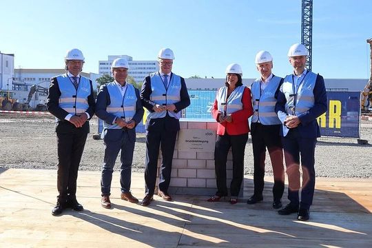
Groundbreaking ceremony at X-Fab in Erfurt in October 2026.
(Image: X-Fab)
X-Fab is also expanding its manufacturing operations at its Erfurt, Germany, facility. In early October 2026, the groundbreaking ceremony for a new cleanroom took place as part of the Fab4Micro project. Unlike the expansion in Sarawak, however, the focus in Erfurt is not on expanding traditional CMOS or BCD capacities, but rather on the production of highly integrated microsystems and photonic solutions. The federal government and the Free State of Thuringia are funding the project with a total of 127.4 million euros under the EU Chips Act. The investment is aimed in particular at applications in the automotive, industrial, and medical technology sectors. Although this does not directly create additional capacity for traditional CMOS or BCD processes, the expansion underscores the strategic importance of specialized semiconductor technologies.
ST is also pursuing a similar specialization. The company is developing its Agrate, Italy, facility into a hub for analog, BCD, smart power, and mixed-signal technologies and is expanding its 300-mm manufacturing operations there. In Germany, Infineon has invested approximately five billion euros (US$5.65 billion) in its Smart Power Fab in Dresden, which opened in July 2026. The facility is slated to manufacture power, analog, and mixed-signal semiconductors. Globalfoundries, for its part, is expanding its Dresden site at a cost of 1.1 billion euros (US$1.243 billion). By the end of 2028, the site is expected to have an annual production capacity of more than one million 300-mm wafers.
Bosch, too, continues to focus on specialized semiconductor manufacturing. At its facility in Reutlingen, Bosch manufactures automotive ICs, MEMS sensors, and power semiconductors, among other products, on 200-mm wafers. The technology portfolio includes both established silicon processes with feature sizes down to 180 nm and SiC power semiconductors.
Of course, a distinction must be made between specialized contract manufacturers and semiconductor manufacturers that rely primarily on in-house production. While foundries such as X-Fab and Globalfoundries also manufacture chips based on external designs, the production capacity of Infineon, STMicroelectronics, and Bosch is primarily used to manufacture their own products.
For device developers, both models can strengthen the supply of components. On the other hand, those who need to have their own ASICs manufactured at another foundry require a contract manufacturer with the appropriate technology. Should that manufacturer ever become unavailable, not every new manufacturing capacity is a viable alternative. Furthermore, the processes cannot be interchanged at will. A new production facility for specific power or mixed-signal technologies cannot simply take over all existing analog, high-voltage, or sensor processes.
More Capacity Does Not Automatically Mean Greater Security of Supply
An additional challenge is the geographic distribution of new capacity. According to Trendforce’s research, Chinese foundries account for approximately 70 percent of the global expansion of established 300-mm processes. This may open up new sourcing options for European customers. At the same time, it raises questions about geographic dependence, supply chain transparency, and the qualification of additional manufacturing partners.
Alongside price pressures in individual manufacturing processes, extensive new capacity for established semiconductor technologies is emerging, particularly in China. The European Commission is therefore warning of potential overcapacity that could put European semiconductor manufacturers under economic pressure. However, this development must be viewed in a nuanced way when it comes to security of supply: The decisive factor is not merely how many additional wafers can be produced, but rather which technologies are available for that purpose. While certain processes could lead to an oversupply, others may remain in short supply. Whether additional capacity actually offers an alternative for European customers therefore depends on the specific manufacturing technologies involved.
Another development at X‑FAB illustrates just how complex switching between manufacturing processes can be. Together with Cadence, the company presented a more highly automated approach to migrating IC designs between process nodes in May 2026. Among other things, they demonstrated the migration of a design from 180 nm to 110 nm. This is because simply reducing the feature size is not enough. Circuit design, layout, and electrical characteristics must be verified for the target technology and adjusted as necessary. This is particularly true for analog and mixed-signal circuits, where the characteristics of the components can directly affect functionality.
The situation is different for companies that use off-the-shelf standard components. They cannot modify the manufacturing process of their ICs themselves, but must rely on the semiconductor manufacturer’s product strategy or suitable alternatives.
What Chips will Europe's Industry Need in the Long Term?
The answer to this question is likely to become even more important in the coming years. A study presented by the ZVEI in May 2026 predicts that the semiconductor demand of the manufacturing industry in Europe will increase by a factor of 2.4 by 2040. At the same time, according to the study, the costs of front-end manufacturing in Germany are, on average, 15 to 30 percent higher than those at the most cost-effective Asian locations.
The expansion of European manufacturing capacity must therefore not only be economically viable but also align with the industry’s actual needs. In addition to high-performance logic chips, this includes analog, mixed-signal, microcontroller, sensor, and power semiconductors, which must remain available for many years to come. It remains to be seen how significantly the price increases observed by Trendforce will actually affect individual component families and electronics development in Germany. It is also unclear to what extent specialty foundries will be able to absorb the capacity shifts of larger competitors.
Foundries, semiconductor manufacturers, distributors, and electronics developers will be surveyed to determine which processes are coming under pressure, where new manufacturing alternatives are emerging, and what consequences this has for the development of durable electronic products.
For while the semiconductor industry continues to set new manufacturing records, another question remains just as important: Who will manufacture the chips that Europe’s industry depends on in the long term?