3-level DC/DC converters offer higher efficiency while requiring less space and costing less. Because this topology uses smaller components, has lower losses, and features a more streamlined bill of materials, it is well-suited for high-power power supplies.
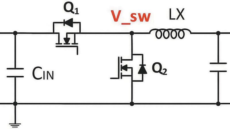
Figure 1: Typical 2-level DC/DC topology.
(Image: Renesas)
Alex Zhou is a Product Marketing Manager at Renesas
Modern power supply systems face two conflicting requirements: higher power output at lower costs. Whether powering next-generation consumer electronics, power tools, or high-power USB-PD applications, developers must integrate more efficient solutions into smaller and more cost-effective designs. One promising solution is the 3-level DC/DC converter architecture. It enables significant efficiency gains, lowers bill of materials (BOM) costs, and reduces PCB size.
Why a 3-level DC/DC Converter?
A 2-level buck controller uses two FETs (external or internal) and a single inductor for power transfer. The topology is referred to as a 2-level buck converter because the switching node alternates exclusively between VIN and ground. In this topology, the FETs must block the full VIN voltage when turned off, and the current ripple across the inductor reaches its maximum at a duty cycle of 50%.
Compared to a conventional two-stage (2L) buck converter, the three-stage (3L) buck converter consists of two additional switches and a flying capacitor. Switches Q1 and Q4 operate out of phase, as do Q2 and Q3.
The switching node (V_SW) alternates between VIN and VIN/2, or between VIN/2 and ground—hence the term “3-level.”
In steady state, the flying capacitor maintains a voltage of V IN /2, which reduces the voltage stress on the switches. This allows the use of FETs with a lower breakdown voltage and a better figure of merit, thereby reducing both conduction and switching losses.
This topology also allows for the use of a smaller inductor, since only half of VIN is applied to it. The current ripple across the inductor occurs at twice the switching frequency of the FETs. As a result, the current ripple (peak-to-peak) is only one-quarter of the value of a 2-level converter, which leads to reduced core losses and lower DCR losses in the inductor.
Opportunities for Reducing the Bill of Materials
By taking advantage of the improved thermal and electrical efficiency of 3-level designs, developers can:
Reduce the size of inductors and capacitors without compromising performance.
Reduce the number of components by using simplified snubber circuits and EMI filtering.
Select MOSFETs with a lower breakdown voltage, which are more cost-effective and have lower conduction losses.
Practical Application Examples
USB-PD Multi-Port Chargers: In high-power USB-PD applications (especially EPR > 65 W), efficiency and thermal management are of critical importance. A 3-level DC/DC converter can operate at higher switching frequencies without compromising efficiency. This enables the use of smaller magnetic components and faster transient response. The reduced heat loss enables slimmer, fanless enclosures and directly lowers manufacturing and material costs.
Power supply products for the consumer market: In products such as laptops, docking stations, and high-end portable audio equipment, space on the printed circuit board is often limited. A smaller power stage not only reduces bill-of-materials costs but also frees up additional PCB space for other functions or reduces the form factor. A power stage architecture that combines a 3-level and a 2-level switching node also enables operation in buck, buck-boost, or boost modes.
Lower Voltage Load
Since each component in a 3-level converter is subjected to a smaller voltage change, the voltage derating requirements are reduced. For example, in a 2-level step-down converter that steps down 24 V to 5 V, the high-side MOSFET must block the full 24 V when turned off. This requires a component with a breakdown voltage of 30 V to 40 V, as well as a higher RDS(on) and higher cost. In a 3-level topology, however, the MOSFET only needs to block about half of this voltage (≈12 V). This allows the use of a MOSFET with a voltage rating of 15 V to 30 V, featuring a significantly lower RDS(on), better switching characteristics, and lower cost.
This effect carries through the entire design: The reduced voltage stress allows designers to select components with lower breakdown voltage and higher power handling. These components often have a better Figure of Merit (FOM) as well as lower conduction and switching losses. The result is a smaller, more cost-effective power stage that generates less heat.
Advantages: Inductance and Efficiency
Since current ripple is inherently lower in a 3-level converter, the requirements for the size of the inductor are also reduced. For example, in a 2-level buck converter that steps down from 24 V to 12 V, the inductor must handle the full voltage change from 24 V to 0 V during each switching cycle. This results in higher current ripple (peak-to-peak), so designers must use larger inductors with a higher core volume and more copper windings. Larger inductors not only increase costs but also result in higher direct-current resistance (DCR). This increases conduction losses and further reduces efficiency.
Date: 08.12.2025
Naturally, we always handle your personal data responsibly. Any personal data we receive from you is processed in accordance with applicable data protection legislation. For detailed information please see our privacy policy.
Consent to the use of data for promotional purposes
I hereby consent to Vogel Communications Group GmbH & Co. KG, Max-Planck-Str. 7-9, 97082 Würzburg including any affiliated companies according to §§ 15 et seq. AktG (hereafter: Vogel Communications Group) using my e-mail address to send editorial newsletters. A list of all affiliated companies can be found here
Newsletter content may include all products and services of any companies mentioned above, including for example specialist journals and books, events and fairs as well as event-related products and services, print and digital media offers and services such as additional (editorial) newsletters, raffles, lead campaigns, market research both online and offline, specialist webportals and e-learning offers. In case my personal telephone number has also been collected, it may be used for offers of aforementioned products, for services of the companies mentioned above, and market research purposes.
Additionally, my consent also includes the processing of my email address and telephone number for data matching for marketing purposes with select advertising partners such as LinkedIn, Google, and Meta. For this, Vogel Communications Group may transmit said data in hashed form to the advertising partners who then use said data to determine whether I am also a member of the mentioned advertising partner portals. Vogel Communications Group uses this feature for the purposes of re-targeting (up-selling, cross-selling, and customer loyalty), generating so-called look-alike audiences for acquisition of new customers, and as basis for exclusion for on-going advertising campaigns. Further information can be found in section “data matching for marketing purposes”.
In case I access protected data on Internet portals of Vogel Communications Group including any affiliated companies according to §§ 15 et seq. AktG, I need to provide further data in order to register for the access to such content. In return for this free access to editorial content, my data may be used in accordance with this consent for the purposes stated here. This does not apply to data matching for marketing purposes.
Right of revocation
I understand that I can revoke my consent at will. My revocation does not change the lawfulness of data processing that was conducted based on my consent leading up to my revocation. One option to declare my revocation is to use the contact form found at https://contact.vogel.de. In case I no longer wish to receive certain newsletters, I have subscribed to, I can also click on the unsubscribe link included at the end of a newsletter. Further information regarding my right of revocation and the implementation of it as well as the consequences of my revocation can be found in the data protection declaration, section editorial newsletter.
In a 3-level buck converter, the effective voltage across the inductor is halved because the switching operations occur between the intermediate levels (≈12 V to 0 V or 24 V to 12 V). This reduces current ripple by nearly 50%, allowing the same level of current ripple to be achieved with a smaller inductor. Smaller inductors with lower DCR result in reduced conduction losses, faster transient response, and a more compact design. At the same time, the lower current ripple reduces the load on the output capacitors and improves system reliability. The result is higher efficiency, a smaller footprint, and lower overall system costs. This makes the 3-level topology particularly attractive for applications with high currents and limited space.
Impact at the System Level
The transition to a 3-level DC/DC architecture is not just a change at the component level; it also has implications for the entire system. These can translate into measurable benefits across the entire product design.
Lower thermal design requirements: Because the 3-level topology reduces switching and conduction losses, less heat is generated in the power stage. For example, in a 200-W USB PD charger, power dissipation can be reduced by 1 W to 2 W compared to a 2-level design. As a result, a bulky aluminum heat sink can be replaced by a smaller, stamped metal part—or eliminated entirely. This eliminates the need for thermal pads or heat pipes and reduces bill-of-materials costs as well as assembly complexity.
Smaller PCB area for power conversion: Thanks to lower losses and reduced voltage stress, inductors and capacitors can be designed to be smaller. In a typical notebook power supply, for example, the area of the power stage can be reduced by 20% to 30%. This frees up valuable space on the PCB, which can be used for additional connectors, wireless charging coils, or an optimized mechanical design. In addition, smaller components enable a more compact design and make it easier to meet specifications regarding enclosure size or weight.
Higher efficiency leads to lower operating costs for the end user: For consumer devices produced in large volumes, efficiency gains of 0.5% to 1% already result in noticeable energy savings over the product’s entire lifespan. For example, a 95% efficient 240 W 3-level USB PD charging adapter operating at full load for eight hours a day loses about 12 W less power than a 93% efficient 2-level design. This reduces both electricity costs and heat generation for the end user. This is particularly relevant in corporate or data center environments where dozens or hundreds of such devices are in use.
Conclusion
The 3-level DC/DC converter is an effective solution for maximizing value in power supply systems. Since bill-of-materials costs are reduced, components are becoming smaller, and thermal management is simplified, developers can use this topology to create high-performance, cost-effective products that meet the demands of modern applications. With the growing demand for USB-PD and other high-power applications, the 3-level approach is becoming increasingly attractive to developers who prioritize both performance and cost-effectiveness.



:quality(80)/p7i.vogel.de/wcms/9e/23/9e23111e49d73012e9e3b7c69428ad5c/0134019347v1.jpeg "The Dominant VA45 high-helix tap from Bass, made of lead-free brass. The long chips, which result from the absence of lead, are clearly visible. (Image:Bass, Inc.)")
:quality(80)/p7i.vogel.de/wcms/1d/09/1d0999956ef87709b72ab1d0402ba207/csf-minis-gruppe-final-01-outputv1.jpeg "Since mid-2026, Harmonic Drive has been offering its CSF Mini gearheads in size 7 as well, in six variants designed for different installation scenarios. (Source: Harmonic Drive)")
:quality(80)/p7i.vogel.de/wcms/ab/08/ab08675922c3a7edea45128248b45b00/0133857009v1.jpeg "In the aerospace industry—one of the most demanding sectors of all—the Shanghai-based company TOPNC has already made a name for itself. (Image:TOPNC)")
:quality(80)/p7i.vogel.de/wcms/ff/48/ff48b1154746e79128935f28bd73ba0e/0113143253v1.jpeg "In our China Market Insider, we regularly provide you with relevant information straight from China. (Image:© Eisenhans - stock.adobe.com)")
:quality(80)/p7i.vogel.de/wcms/89/01/890193a30c52ffd4811d18db82170952/0113143253v1.jpeg "In our China Market Insider, we regularly provide you with relevant information straight from China. (Image:© Eisenhans - stock.adobe.com)")
:quality(80)/p7i.vogel.de/wcms/6b/8a/6b8ac7cd85db2d1d1f6ab30957648711/schaeffler-news-taicanglighthouse6v1.jpeg "At the Lighthouse Factory, robots assemble linear and rotary actuators, among other components. (Source: Schaeffler)")
:quality(80)/p7i.vogel.de/wcms/4f/5a/4f5a2417df55dae5967e90b331e0bbc5/physical-ai-robotics-ariv1.jpeg "With new hardware and software solutions, the productive use of AI in industry is becoming increasingly prominent. (Source: Nvidia)")
:quality(80)/p7i.vogel.de/wcms/ba/d6/bad6e38e53c7443934b4c9a5a70e14d7/a264823-largev1.jpeg "At the Production Lab, where Audi tests future technologies for production and logistics, mobile humanoid robots from Agile Robots retrieve parts from material bins and place them in sequence carts. (Audi AG)")
:quality(80)/p7i.vogel.de/wcms/c3/68/c368b4f6821557ec497c64bc17fe9f8d/adobestock-2051843806--kaliel-stock-adobe-com-ki-generiertv1.jpeg "To truly harness the full potential of virtual product development, teams and management must radically change their mindset. (Source: © kaliel – stock.adobe.com_AI-generated)")
:quality(80)/p7i.vogel.de/wcms/a3/c1/a3c19e028b66a6fd7c373ab94981631d/paprika-gripperv1.jpeg "For the final, additively manufactured gripper base, SoftGripping chose PA 2200, a material based on polyamide 12 (PA12). It offers balanced mechanical properties and high load-bearing capacity, making it ideal for robust gripper solutions with integrated pneumatics. (Source: SoftGripping GmbH)")
:quality(80)/p7i.vogel.de/wcms/51/b8/51b8e08d2105fdd9952aff385f154192/graphic-2-adma1v1.png "The new surface hardening process enhances the performance of corrosion-resistant alloys by improving their tribological and mechanical surface properties, while preserving the properties of the base material. (Source: Bodycote)")
:quality(80)/p7i.vogel.de/wcms/96/ef/96effc239916cb7e0f396ab75627b8c0/image-space-testingv1.jpeg "Two scientists in front of a vacuum chamber used for testing: As technical instruments for spaceflight become more sensitive, the test facilities are becoming a critical system. (Source: Busch Group)")
:quality(80)/p7i.vogel.de/wcms/ba/d3/bad3d62389a59fe3cdbac386a0dce64b/0134098250v1.jpeg "Following initial tests with its robotaxis in Europe, Pony.ai now plans to bring robot trucks to Europe as well. (Image:Pony.ai)")
:quality(80)/p7i.vogel.de/wcms/78/d1/78d124651f6149aa9f33913fc00ef98a/bertrandt-standort-tschechienv1.jpeg "Bertrandt has opened a new facility in the Czech Republic—near Škoda. (Source: Bertrandt)")
:quality(80)/p7i.vogel.de/wcms/03/9b/039b002b36a5983bb1bb0fefafcdf3dc/0134083586v1.jpeg "After Volkswagen announced last week that many electric cars of various models worldwide would have to be recalled due to battery problems, the specific number of affected vehicles has now been determined. In Germany, the number is around 10,000 ... (Image: Volkswagen)")
:quality(80)/p7i.vogel.de/wcms/3a/0b/3a0b7a7fc3898a25a0c849690d641390/0134084456v1.jpeg "After Elon Musk had previously been rather cautious in his comments about a long-discussed merger between Tesla and SpaceX, things now seem to be taking shape—or so it appears... (Image: Tesla)")
:quality(80)/p7i.vogel.de/wcms/cd/23/cd239aa506b3ace30e62f44c83fa31ca/0134051508v1.jpeg "Figure 1: Schematic representation of the DAB (Dual Active Bridge) topology. (Image:Texas Instruments)")
:quality(80)/p7i.vogel.de/wcms/8b/35/8b35660420abba32fb891a4c5cc42fbd/0134018092v1.jpeg "Long-range UVC LED with lens and reflector: Close-up of a square LED with a transparent, dome-shaped lens on a dark base plate. The hermetically sealed housing ensures greater reliability and durability under demanding environmental conditions. (Image:FBH_Schurian)")
:quality(80)/p7i.vogel.de/wcms/a4/1c/a41cd52e0a26e5173bd4e1f834d4f7f4/0134025034v1.jpeg "As chips become more complex, the demands on semiconductor testing increase. Teradyne and FormFactor plan to combine their technologies for future applications. (Image:freely licensed)")
:quality(80)/p7i.vogel.de/wcms/7b/64/7b64e9fe595b88d2b01ed79e0f2baf94/pm-weidm-ller-elatec-substation-line-switchv1.jpeg "Caption: The Substation Line managed switches can accommodate up to three HSR/PRP modules. (Image:Weidmüller)")
:fill(fff,0)/images.vogel.de/vogelonline/companyimg/76800/76895/65.jpg "FAULHABER_120mm.jpg ()")
:quality(80)/p7i.vogel.de/wcms/e1/4d/e14df70b29c4f3729b77c0dc1664ef63/0132282816v1.jpeg "Figure 3: Current ripple across the inductor versus duty cycle for 2-level and 3-level buck converters.(Image: Renesas)")
:quality(80)/p7i.vogel.de/wcms/88/f3/88f3f36a3312d6752c21960f526fd4a4/0132282852v1.jpeg "Figure 4: Block diagram of a USB PD multi-port charger with a 3-level DC/DC converter.(Image: Renesas)")
:quality(80)/p7i.vogel.de/wcms/28/32/283239c22550727063ede0b1d9b6907a/0132283069v1.jpeg "Figure 5: Diagram of a consumer-grade power supply product with a 3-level DC/DC converter.(Image: Renesas)")
:quality(80)/p7i.vogel.de/wcms/2c/be/2cbe71b3d79ba5b3241c3a380d190718/0132282528v1.jpeg "Figure 1: Typical 2-level DC/DC topology.(Image: Renesas)")
:quality(80)/p7i.vogel.de/wcms/2f/19/2f1928ea68e2cf840ebba6313fc08201/0133462125v1.jpeg "Converters: Integrated GaN buck and boost converters for the medium-voltage range require 50% less space than silicon-based alternatives, without compromising efficiency. (Image:TI)")
:quality(80)/p7i.vogel.de/wcms/82/53/8253c7a38b4891e5822a06405e0124cb/0129319571v1.jpeg "The losses and penetration depth depend on the frequency. (Picture: ©studioworkstock - stock.adobe.com)")