Design Flow Adjustments for New Performance LimitsThe 2-Nanometer Process and the Performance Trap
By
Filipe Martins and Anna Kobylinska* | Translated by AI
12 min Reading Time
The exploding demand for AI chips is driving the expansion of fabs for advanced nodes to unprecedented heights—moving towards 12-inch wafers. While the semiconductor industry invests in new 12-inch fabs, older 6-inch production facilities in Europe are increasingly losing significance.
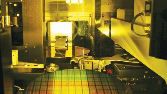
FOUP wafer cassette for 300-mm semiconductor manufacturing in TSMC's Fab 12.
(Image: TSMC)
At 2 nm, semiconductor manufacturing has reached a point where further miniaturization of structures alone no longer guarantees reliable performance gains. Gate-all-around transistors improve density and energy efficiency, but resistances, parasitic capacitances, power supply, manufacturing variations, and heat dissipation slow progress at the chip and system level.
Autonomy – robotics, driving, and flying – requires the 2-nm node. In the image: Qualcomm manager Nakul Duggal with a humanoid robot from Neura Robotics based in Metzingen.
(Image: Qualcomm)
Since around the 22-/28-nm generation, the nanometer number in the name no longer corresponds to any measurable physical structure on the chip—neither to the gate length nor to any other dimension. For example, Intel's current "10 nm" corresponds in density more to TSMC's and Samsung's "7 nm," and the "Angstrom era" (20A, 18A) uses the letter A to suggest a scale of about 2 nm, without referring to any actual angstrom dimension. The IEEE itself points out in its International Roadmap for Devices and Systems (IRDS) that the projected physical parameters should be understood independently of the node naming conventions of individual foundries. The relevant geometrical dimensions Contacted Poly Pitch (CPP), Minimum Metal Pitch (MP), and Cell Height are not standardized between TSMC, Intel, and Samsung—"2 nm" from three manufacturers can correspond to three different CPP/MP combinations.
So, equating "2 nm" with a specific level of technical maturity is, in reality, comparing apples to oranges. Moreover, the discrepancy in the actual performance of various chip designs in 2-nm process nodes also stems, not least, from decisions regarding wiring and power supply.
Same But Different
The three leading logic foundries are adopting GAAFET (Gate-All-Around Transistors) in their latest leading-edge generations, replacing FinFET in the most advanced processes. TSMC calls its variant Nanosheet, Samsung refers to it as MBCFET (Multi-Bridge-Channel-FET), and Intel uses the term RibbonFET. TSMC and Samsung associate this transistor generation with their 2-nm nodes, N2 and SF2; Intel markets the comparable architecture under the designation 18A.
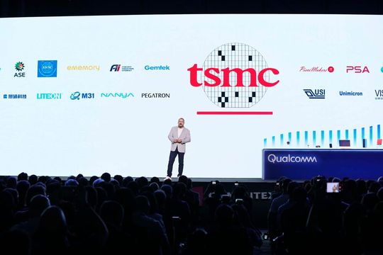
Agentic AI drives the demand for energy-efficient computing power at the edge – in 2-nm manufacturing. In the image: Qualcomm CEO Cristiano Amon at Computex 2026.
(Image: Qualcomm)
Technically, it involves three variations of the same principle: The gate surrounds the channel on all sides, improving electrostatic control and giving the transistor flexibility in performance, leakage current, and scaling—at least at the component level. In design practice, a different picture emerges: The 2-nm node does not automatically result in a faster chip.
A reliable single metric for the 2-nm process node is the actual transistor density in millions of transistors per mm² (MTr/mm²) for a defined standard cell mix. According to Techinsights analyses of the IEDM/ISSCC papers, the high-density logic density is around 313 MTr/mm² for TSMC N2, approximately 238 MTr/mm² for Intel 18A, and about 231 MTr/mm² for Samsung SF2/SF3P. This figure strongly depends on the assumed cell mix (logic/SRAM/analog) and is only partially comparable between foundries unless the semiconductors are based on exactly the same cell configuration.
Because logic density heavily depends on design, the industry has long used the SRAM bit cell area as a relatively objective maturity indicator, as SRAM arrays are highly standardized. Manufacturer specifications for performance/power/area (e.g., TSMC's "15% higher clock speed or 30% lower power consumption compared to N3E") come from IEDM papers with real test chips and ring oscillator measurements, so they are not purely speculative. Cross-vendor rankings, however, become problematic: they are based on foundry metrics and an extrapolation method rather than on actual silicon measurements using identical test circuits.
Actual yield data is almost never officially published; more reliable are indirect signals, including HVM discipline, the number of confirmed customer tape-outs, capacity commitments, actual wafer deliveries, and the variability of process parameters (Vt-sigma) across multiple production lots.
Even a physically completed process is unusable without a design ecosystem. Evaluation criteria include:
PDK certification status with major EDA providers (as described in the article using Siemens EDA/Calibre for TSMC N2/A16 as an example),
Completeness of the IP libraries (memory compilers, high-speed SerDes, analog IP),
Availability of multi-project wafer shuttles for smaller customers,
Number and maturity of sign-off corners (corner models) that allow reliable statements about timing closure under real manufacturing variations.
Lacking reliable reference values, design teams face a tough choice. A number of 2-nm-specific challenges bring additional surprises.
Switching and ... Waiting
The undisputed performance gain of the GAAFET transistor dissipates on the way to the finished chip due to a series of gradual losses and a cascade of accumulated bottlenecks: in local and global wiring, the power supply network, placement and routing congestion, voltage and temperature variation—and ultimately in the sign-off.
The PPA (Power, Performance, Area) values communicated by the foundries are aggregate figures derived from foundry-defined test chips, reference blocks, and operating points. They cannot be directly translated into reliable timing or power budgets for a specific product. TSMC states for N2, compared to N3E, a 10 to 15 percent performance increase at the same power consumption or 25 to 30 percent lower power consumption at the same performance, as well as 15 percent higher chip density—this should not be confused with the "transistor density" often cited in secondary sources.
Date: 08.12.2025
Naturally, we always handle your personal data responsibly. Any personal data we receive from you is processed in accordance with applicable data protection legislation. For detailed information please see our privacy policy.
Consent to the use of data for promotional purposes
I hereby consent to Vogel Communications Group GmbH & Co. KG, Max-Planck-Str. 7-9, 97082 Würzburg including any affiliated companies according to §§ 15 et seq. AktG (hereafter: Vogel Communications Group) using my e-mail address to send editorial newsletters. A list of all affiliated companies can be found here
Newsletter content may include all products and services of any companies mentioned above, including for example specialist journals and books, events and fairs as well as event-related products and services, print and digital media offers and services such as additional (editorial) newsletters, raffles, lead campaigns, market research both online and offline, specialist webportals and e-learning offers. In case my personal telephone number has also been collected, it may be used for offers of aforementioned products, for services of the companies mentioned above, and market research purposes.
Additionally, my consent also includes the processing of my email address and telephone number for data matching for marketing purposes with select advertising partners such as LinkedIn, Google, and Meta. For this, Vogel Communications Group may transmit said data in hashed form to the advertising partners who then use said data to determine whether I am also a member of the mentioned advertising partner portals. Vogel Communications Group uses this feature for the purposes of re-targeting (up-selling, cross-selling, and customer loyalty), generating so-called look-alike audiences for acquisition of new customers, and as basis for exclusion for on-going advertising campaigns. Further information can be found in section “data matching for marketing purposes”.
In case I access protected data on Internet portals of Vogel Communications Group including any affiliated companies according to §§ 15 et seq. AktG, I need to provide further data in order to register for the access to such content. In return for this free access to editorial content, my data may be used in accordance with this consent for the purposes stated here. This does not apply to data matching for marketing purposes.
Right of revocation
I understand that I can revoke my consent at will. My revocation does not change the lawfulness of data processing that was conducted based on my consent leading up to my revocation. One option to declare my revocation is to use the contact form found at https://contact.vogel.de. In case I no longer wish to receive certain newsletters, I have subscribed to, I can also click on the unsubscribe link included at the end of a newsletter. Further information regarding my right of revocation and the implementation of it as well as the consequences of my revocation can be found in the data protection declaration, section editorial newsletter.
The N2 maturity is demonstrated, among other things, by a logic test chip with more than three billion gates and an SRAM test chip with over 90 percent yield after 1,000-hour HTOL qualification. While these are reliable, they are product-distant proofs without guaranteeing a real SoC with its own power grid and individual operating profile. Anyone who adopts foundry KPIs unchecked into a project timing budget risks encountering negative slack or unexpected power integrity issues, especially during the first sign-off run.
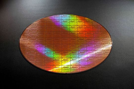
Rapidus has begun prototype production of 2-nm GAA transistors at the IIM-1 facility in Chitose. Illustration: Prototype of a 2nm Gate All Around Transistor on a silicon wafer.
(Image: Rapidus)
Even the manufacturing maturity itself remains classified: TSMC does not release an official yield figure for the N2 launch; in the trade press, unconfirmed estimates of 70 to 80 percent were circulating for the early ramp. For Samsung's SF2, industry estimates paint a similarly incomplete picture: around 50 percent at the production start of the Exynos 2600 in September 2025, and, according to a report from early August 2026, now around 60 percent—70 percent is considered in the industry as the threshold at which large customer contracts can be economically transitioned into mass production.
The real reason for the growing decoupling of node designation from actual chip performance lies in the physics of interconnects.
With each scaling step, the cross-section of the copper interconnects shrinks, while their electrical resistance increases disproportionately: barrier and liner layers occupy a growing share of the already limited conductor cross-section, and electron scattering at surfaces and grain boundaries further amplifies the resistance increase. As a result, a growing portion of path delay no longer originates in the gate but in the interconnect itself—RC delay becomes a central determinant of timing.
Concrete, node-specific metal pitch values for current N2, SF2, and 18A implementations are not published by the foundries; the BEOL geometry remains largely proprietary. The general physical assertion that sub-20 nm metal pitches become relevant for continued scaling beyond the 2 nm class is reliable, but this is a different statement from a direct, cross-foundry pitch specification for today's 2 nm processes.
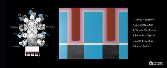
Applied Materials extends copper interconnects to 2 nm and subsequent smaller nodes with its new Integrated Materials Solution.
(Image: Applied Materials)
Material development is accordingly focused on thinner yet equally effective diffusion barriers and liners. In 2024, Applied Materials introduced a Ruthenium-Cobalt (RuCo) liner, reducing the liner thickness to less than 20 angstroms—about one-third less than previous solutions. This increases the cross-section available for copper; according to the manufacturer, the line resistance is reduced by up to 25 percent. Applied Materials states that this technology is already in use by leading logic manufacturers and has been qualified since the 3 nm generation, displacing established barrier and liner stacks made of tantalum nitride (TaN) and cobalt in critical metal layers. Seedless copper deposition and new dielectrics complement this: they improve the seamless filling of narrow interconnects, enhancing their electrical reliability.
Power Supply as a Bottleneck
In traditional frontside power delivery, the signal and power supply networks compete for the same BEOL metal layers. The narrower and longer a power delivery path is, the greater its ohmic voltage drop—known as IR drop—between the power input and the transistor. The consequences range from longer cell delays and shifted clock arrival times to timing violations in PVT corners that were still uncritical with higher voltage margins.
Backside Power Delivery Networks (BSPDN) relocate the power supply network to the backside of a heavily thinned wafer, thereby physically separating it from the signal wiring. This shortens the supply paths, and their resistance can be significantly reduced; Semianalysis estimates the effect at roughly an order of magnitude.
The three foundries are making this architectural shift at different times. TSMC keeps N2 and N2P on frontside power, while A16 introduces backside power and remains, according to a TSMC VLSI technical paper (June 2026) and a report from August 13, 2026, scheduled for the fourth quarter of 2026. Intel has already implemented it with PowerVia in 18A production, while the timeline for Samsung's SF2Z remains unclear.
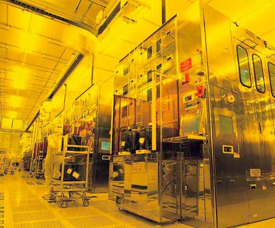
Manufacturing facilities of TSMC for 300-mm (approx. 11.8-inch) wafers.
(Image: TSMC)
Design consequence: The foundry choice automatically determines the power delivery architecture and the timing from which IR-drop constraints structurally ease floorplanning.
The specific requirements differ significantly depending on the implementation approach. IMEC's nTSV/BPR concept requires extreme wafer thinning to a few hundred nanometers of residual silicon and an overlay accuracy better than 10 nm between the backside via and the power rail. Direct-contact architectures, where the backside metallization is directly connected to gate or source/drain structures, demand an even tighter overlay budget of around 3 nm.
On the thermal side, IMEC has determined through high-resolution simulations of a cloud CPU SoC architecture a potential local temperature increase of up to 14 degrees Celsius (approx. 25 degrees Fahrenheit) compared to traditional frontside power delivery, as the thin residual silicon layer largely fails as a lateral heat spreader. Power, timing, and thermal sign-off must therefore be treated as a coupled optimization process; they can no longer be approached sequentially.
Variation as a Sign-Off Risk
GAAFET transistors introduce their own dimension of variability: backside metallization and the nano-TSVs required for direct-connect BSPDN create mechanical stress profiles that can impact channel strain, charge carrier mobility, and thus the drive current of the nanosheet channels—varying in intensity depending on transistor position and chip layout. Modern sign-off flows account for this through layout-dependent timing variation and layout proximity effects.
On the electromigration side, a statistical component comes into play: identical metal lines with the same geometry and load can show different time-to-failure values due to variations in grain sizes and crystal orientations. In EM research, a resistance increase of around ten percent compared to the initial value is often used as a failure criterion—this is a common measurement convention but not a universal sign-off threshold. As metal cross-sections shrink and current density increases, the expected EM lifetime continues to decrease, intensifying the trade-off between performance and reliability—especially in 3D integration with its residual mechanical stresses.
Sign-Off Not as Expected, But Reimagined
For design teams, this results in a clear consequence: timing, power, and reliability sign-off must begin early at 2 nm, be tightly integrated, and take place in short iterations—not late and sequentially. However, the degree of this coupling depends on a number of variables, including the product class, library, PDN architecture, and the respective reliability targets.
A concrete example shows how this is reflected in the layout.
TSMC's NanoFlex technology, introduced with N2, is not a variation of nanosheet width but rather flexibility in standard cell architecture: within the same functional block, short cells with minimal area and high energy efficiency can be combined with tall cells for maximum performance, instead of making a uniform compromise for the entire block.
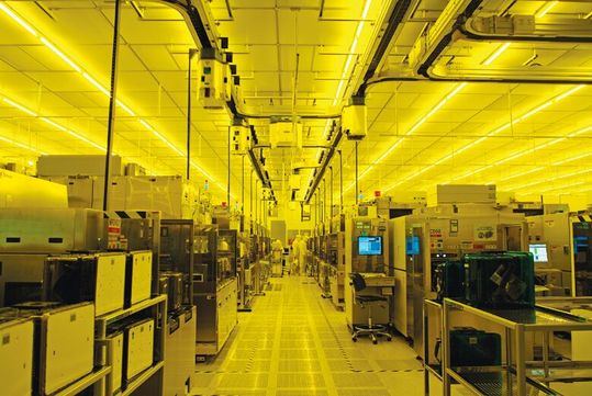
Inside a manufacturing hall of TSMC
(Image: TSMC)
Cadence has aligned its implementation tools with N3, N2, A16, and A14, with the further developed Nanoflex Pro variant for A14 as a focal point. The goal is to harmonize front-end placement and back-end routing rules to improve the correlation between pre-route and post-route timing. This serves as a direct lever against late sign-off surprises caused by congestion and RC misestimations.
Practical consequence: A floorplan team must determine during block partitioning which areas will receive short cells for energy efficiency and which will receive tall cells for clock frequency—this directly impacts power grid dimensioning, macro placement, and subsequent IR-drop and timing sign-off. With A16, a second effect comes into play: the super-power rail architecture shifts power networks to the backside of the chip, allowing frontside metal layers to be used more densely for signal routing—a routing reserve that floorplanning teams should account for as early as the architecture planning stage.
Roadmaps vs. Implementation
The gap between roadmap announcements and production-ready design flow remains real but is constantly changing. N2 has been in volume production since Q4 2025 and, according to market observers, started with an initial yield of around 70 percent at TSMC sites in Hsinchu and Kaohsiung; N2P will follow in the second half of 2026. A16 is still scheduled for Q4 2026, as outlined above.
TSMC has additionally extended its roadmap to 2029 with N2U, A14, as well as their derivatives A13 and A12 – mostly incremental gains in performance, efficiency, and density, with A12 as the second backside power generation for AI workloads.
Design consequence: EDA certifications lag behind such roadmap announcements. Synopsys and Cadence expanded their collaboration with TSMC to include N3, N2, A16, and A14 in April 2026, but PDK alignment for A14 is still ongoing—currently, only N2 and A16 are fully certified. The sign-off challenge is therefore not resolved but shifts to the next node generation.
How inconsistent "certified" can be is illustrated by a German example: Siemens EDA, the EDA business unit of the Munich-based Siemens Group that emerged from the 2017 acquisition of US provider Mentor Graphics, already certified its Calibre nmPlatform tool for physical verification (DRC/LVS) for TSMC's N2 in 2023 and additionally for A16 and A14 in April 2026. Synopsys and Cadence, on the other hand, have fully certified only their implementation and sign-off flows up to A16; for A14, PDK alignment is still ongoing. For design teams, this means that "certified" often applies only to specific tool classes, not automatically to the entire flow—before starting a project, it is worth checking the certification status of each individual tool.
Samsung's situation remains dynamic as well: in August 2026, the foundry revised its roadmap, postponing the 1.4-nm process SF1.4 from its original 2027 target to 2029, and is focusing in the meantime on the differentiation of the SF2 family. For the German automotive industry, this is not an abstract roadmap plan: the supplier Continental already formed a strategic partnership with the US chip manufacturer Ambarella in 2023 for driver assistance and automation systems, with series production starting in 2027.
Ambarella reportedly was among the early customers of Samsung's 2-nm automotive process SF2A. In Samsung's latest publicly available 2-nm roadmap from summer 2026, the designation SF2A, as well as SF2Z with BSPDN, is absent, and Ambarella itself now refers to the taped chip only as a "semi-custom" design.
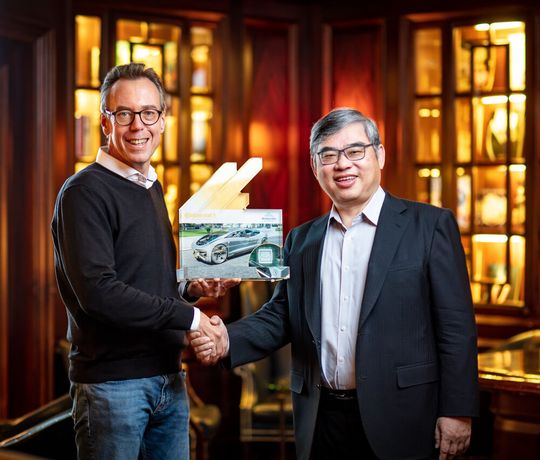
Philipp von Hirschheydt, CEO of Continental Automotive (left), and Fermi Wang, President and CEO of Ambarella, sealed their partnership for AI-powered driver assistance systems – almost three years ago.
(Image: Continental)
Ambarella has already brought its first 2-nm design to tape-out at Samsung (confirmed in Ambarella's CES investor update from January 2026 and in the 10-K annual report). Whether and in what form SF2A will actually be introduced remains uncertain. Delays in its qualification or ramp-up could affect the availability of future automotive SoCs and impact the series production schedules of German suppliers.
On July 25, 2026, Samsung and Broadcom announced a collaboration expected to exceed 200 billion US dollars and run until 2030. It includes advanced packaging technologies such as 2.3D and 2.5D.
In July, Samsung agreed to a collaboration with Broadcom, expected to exceed 200 billion US dollars and run until 2030; Broadcom's upcoming high-speed communication chips are to be manufactured in Samsung's sub-2-nm technology. In the illustration: Samsung Digital City Suwon.
(Image: Samsung)
For a specific project, the node alone is not decisive, but whether and when the chosen process platform provides backside power with the required IP, library, and capacity maturity. Additionally, the interplay of yield, HBM availability, and advanced packaging in the necessary volume plays a critical role.
At 2 nm, the node designation says little about the actual achievable chip performance. The physical limits have shifted from gate length to the metal layers and power delivery network: increasing interconnect resistivity, IR-drop-driven timing violations, and a growing number of statistical variability sources increasingly determine what a design can actually achieve.
Backside power delivery is the most important architectural response to this shift, but it brings its own sign-off complexity in the form of new thermal, mechanical, and overlay constraints—and it is introduced at different times and in different order by the three major foundries.
Anyone looking to bring a 2 nm design to silicon must adjust timing budgets, floorplanning, and sign-off strategies to the new physical bottlenecks. Timing, power, and reliability sign-off should begin earlier in the flow, be more closely integrated, and, where reliability requirements demand it, calculate in a variation-aware rather than purely deterministic manner. Those who make these adjustments can unlock the real PPA advantages of 2 nm. Those who rely on foundry metrics risk falling into the performance trap.
*Anna Kobylinska and Filipe Pereira Martins work for McKinley Denali, Inc., USA.



:quality(80)/p7i.vogel.de/wcms/14/43/1443db59695f7eed2a338d16d03a6257/26-09-30-st-ber-ab-hunger-games-bild-1v1.jpeg "For “The Hunger Games: On Stage,” drive systems lift and move grandstand sections with a dynamic load of up to 26 metric tons—each section can accommodate up to 112 spectators. (Source: Troubadour at the Canary Wharf Theatre)")
:quality(80)/p7i.vogel.de/wcms/5f/96/5f9606264f35f5979529286a887bbccf/0133859498v1.jpeg "Trumpf Expands Its Portfolio for 2D Laser Cutting (Image:TRUMPF GMBH + CO. KG)")
:quality(80)/p7i.vogel.de/wcms/6d/76/6d7682de33991e539956ed72f7d246a3/vibro-cutv1.jpeg "Hybrid machining uses ultrasonic and oscillation technologies to support traditional machining processes. (Source: VibroCut)")
:quality(80)/p7i.vogel.de/wcms/ed/78/ed786ed6b280ff6c692908f01f715e3d/0113143253v1.jpeg "In our China Market Insider, we regularly provide you with relevant information straight from China. (Image:© Eisenhans - stock.adobe.com)")
:quality(80)/p7i.vogel.de/wcms/87/88/8788e0b7fd98cca21a9c370ed0f0aa18/0133859688v1.jpeg "The software newly developed at Fraunhofer IWU helps employees reliably
identify parts that do not meet quality requirements. (Image:Fraunhofer IWU)")
:quality(80)/p7i.vogel.de/wcms/a8/0d/a80d9eb978dd47dbd8f390181a039bfc/adobestock-2081783940--design-store-stock-adobe-com-ki-generiertv1.jpeg "We’re showcasing five of the latest innovations for virtual commissioning—from AI copilots and smart browser tools to deep PLC integration. (Source: © Design Store – stock.adobe.com_AI-generated)")
:quality(80)/p7i.vogel.de/wcms/4b/7c/4b7c11f510878f154012d04c18a7c3cc/0133798118v1.jpeg "RobCo Becomes a Unicorn: The Munich-based robotics company has reached a valuation of more than one billion U.S. dollars and is driving the next generation of autonomous industrial robotics with Alfie. (Image:RobCo)")
:quality(80)/p7i.vogel.de/wcms/c8/a9/c8a96d5841d508c9e9c609c64168cbaa/0133758997v1.jpeg "Hospital Robotics: Neura Robotics' autonomous healthcare platform is designed to independently transport empty hospital beds between wards and floors. (Image:Neura Robotics)")
:quality(80)/p7i.vogel.de/wcms/8a/c8/8ac8eb7fc2b70f4b72771548e2e2e520/epfl-motor-3v1.jpeg "FiberMotor has a diameter of 1 to 3 mm and consists of two concentric hollow fibers. Each fiber is wrapped in tightly insulated copper wire electrodes that are only slightly thicker than a human hair. (Source: EPFL)")
:quality(80)/p7i.vogel.de/wcms/a7/8a/a78a582a42a96aaaff38bd6b8f97a015/vishal-lal-mit-kernuhrv1.jpeg "It's ticking: Researchers have stabilized the first atomic clock. (Source: PTB)")
:quality(80)/p7i.vogel.de/wcms/36/f9/36f96a206fc408c9a632ce849de1f7fa/newsimage428299v1.jpeg "Polystyrene is used in protective packaging for televisions and electronic devices, in decorative moldings and baseboards for interior home construction, and even in Petri dishes. (Source: Hereon/Marcel Schwickerath)")
:quality(80)/p7i.vogel.de/wcms/90/30/90300137452b00d22f95113eff065ac3/fliehkraftkupplungen-und-bremsen-montage-centrifugal-clutches-and-brakes-assembly-1v1.jpeg "Installation: Centrifugal clutches should always be precisely matched to the machine. (Source: Amsbeck Machine Technology)")
:quality(80)/p7i.vogel.de/wcms/50/23/5023ffaefac8f9a47286b368143b88eb/0133801078v1.jpeg "Life isn't exactly a walk in the park for Porsche right now. And now Porsche management is saying that next year will be even worse. Read here to find out why that's supposed to be the case... (Image: Porsche)")
:quality(80)/p7i.vogel.de/wcms/2f/ab/2fabf62cdd2f57cb279e00931c91c869/0133794991v1.jpeg "The Atto 2 SUV is one of BYD's most popular plug-in hybrids. (Image:BYD)")
:quality(80)/p7i.vogel.de/wcms/e9/6e/e96e34d467ca1017f2a689275ae07302/0133815122v1.jpeg "Porsche CEO Leiters has shared new information about the company's model plans. (Image:Porsche)")
:quality(80)/p7i.vogel.de/wcms/0a/50/0a50938be0b598b36efc4e5457ed56dd/forvia-siege-zen-massage-16-9-06v1.jpeg "Seat with massage function by Forvia. (Source: Forvia)")
:quality(80)/p7i.vogel.de/wcms/c6/58/c6581a191008d282eea182627b061e19/0133849717v1.jpeg "Expansion of Manufacturing Operations in the Philippines: Nexperia is expanding its production capacity at its Cabuyao facility to stabilize the semiconductor supply following the loss of control over its Chinese plants. (Image:Nexperia)")
:quality(80)/p7i.vogel.de/wcms/4d/eb/4debf44ac7c0349544c70033bb9a182c/0133750488v1.jpeg "AI-enabled hardware: is a prerequisite for successful AI projects. (Image:Tung Lam)")
:quality(80)/p7i.vogel.de/wcms/36/f0/36f0472d20227013871aa790f4d48ac6/0133726018v1.jpeg "Ion beams can ablate, coat, or smooth surfaces down to the atomic level. Such processes are used, among other things, in optical chips, precision optics, and superconducting materials. (Image:AI-generated)")
:quality(80)/p7i.vogel.de/wcms/1f/47/1f47da6ee12c38a745eb478a04157a65/0133726100v1.jpeg "The schematic diagram shows the structure of a 3D NAND memory device with memory cells stacked on top of one another and vertical connections for high storage density. (Image:Dall-E / AI-generated)")

:quality(80)/p7i.vogel.de/wcms/87/a9/87a9090f5df0a6e1e241ec5e60570e69/0132228435v1.jpeg "With an ambitious pricing strategy, Rapidus, still a relatively young company as a contract manufacturer, aims to directly challenge the dominant competitor TSMC from Japan. However, apart from the technological race, the targeted goal heavily depends on customer demand and investments from the Japanese government. (Image: Rapidus)")

:quality(80)/p7i.vogel.de/wcms/9c/5a/9c5a68d580224bc84742336a0fc89d9f/0132805637v1.jpeg "GM exits the SynergyCells joint venture with Samsung SDI. However, both companies plan to jointly work on a prismatic battery cell. (Image:Samsung SDI)")
:quality(80)/p7i.vogel.de/wcms/c2/a8/c2a8a93f306c1475489dff074ad59731/0129967672v1.jpeg "Figure 1: Imec's logic technology roadmap showing the extension of the nanosheet era from 2nm to the A10 node with the outer-wall forksheet, before the transition to CFET for A7 and beyond. (Image:imec)")
:quality(80)/p7i.vogel.de/wcms/1a/bf/1abf6e3b862a9ba71914b9ef7dce0ca4/0132761112v1.jpeg "Semiconductor scaling: TSMC's roadmap reveals a fundamental shift. Development is no longer solely determined by transistor density, but scaling is moving from the individual chip to the system level. (Image:TSMC)")