


:quality(80)/p7i.vogel.de/wcms/21/b6/21b61c2ac1df28254fb0dad1574fb2d7/0132853015v1.jpeg "The rose-gold, TiAlSiN-based coating material InoxaCon contributes significantly to the stability and service life of HPTec's new RQR-350 milling tool. It enables safe and efficient automated processes in the manufacturing of surgical instruments. (Image:Cemecon)")
:quality(80)/p7i.vogel.de/wcms/d2/73/d273374d6347651e4e6200cf6061ea4e/0132860560v1.jpeg "Even in July, the flag of the Chinese economy did not flutter particularly briskly in the air. Read here what’s happening and why production in China is apparently declining ... (Image:AI-generated)")
:quality(80)/p7i.vogel.de/wcms/18/47/1847f131e3afda201d1dbb98ad0ecb04/0132826776v1.jpeg "Image 1: Difender armored steels from Dillinger stand out with top scores in ballistic testing and cold bending. Defense companies therefore readily choose them. They can be found, for example, in the armored vehicles Fuchs and GTK Boxer of the German Armed Forces. (Image: Dillinger)")
:quality(80)/p7i.vogel.de/wcms/1e/7d/1e7d651782e0e97b3efc25abf2b52350/img-3485v1.jpeg "The Siemens Energy employees attach balancing weights at the precisely calculated and adjusted angular position to achieve the best possible result. (Source: Schenck Rotec)")
:quality(80)/p7i.vogel.de/wcms/a7/38/a73840cb81da9dc3c503f4c04bf66b96/0132892768v1.jpeg "Unitree's IPO symbolizes the high expectations for humanoid robots and embodied AI. (Image:Dall-E / AI-generated)")
:quality(80)/p7i.vogel.de/wcms/1c/a5/1ca5e3ef5d834c3a42de8909c872e3c6/0132876444v1.jpeg "The autonomous transport system Active Shuttle marketed by Bosch Rexroth has been sold to Neura Robotics. (Image:Bosch Rexroth)")
:quality(80)/p7i.vogel.de/wcms/30/1a/301a1aa59e093d848b69e9ff7006b83e/image1v1.jpeg "Wireless switching devices offer advantages in numerous industrial applications – wherever wired communication reaches its limits (Image: Steute) (Image:)")
:quality(80)/p7i.vogel.de/wcms/a2/85/a285b12508af812e28b17be3482a736c/0132488872v1.jpeg "NIS2 is no longer an abstract requirement in the distant future for many industrial companies. (Image:AI-generated)")
:quality(80)/p7i.vogel.de/wcms/41/fc/41fc456ff1ff8f30807924663e8df127/img-0942v1.jpeg "In industrial additive manufacturing, the production strategy must influence the design from the very beginning. (Source: Materialise)")
:quality(80)/p7i.vogel.de/wcms/44/fe/44fe86a16c26c09bb363b3671bf0b930/0132847771v1.jpeg "CoreTechnologie (CT) points out that the 3D printing software 4D_Additive has been equipped with additional application possibilities. Here you can learn more about what the new version 1.8 can do – such as generating complex lattice structures or optimizing faulty data ... (Image:CT)")
:quality(80)/p7i.vogel.de/wcms/b4/f2/b4f2c272247f79c5e87334a6839f20cb/0132549860v1.jpeg "Morefire analysis: Many mechanical engineering websites focus on technical specs instead of customer benefits. Translating features into clear benefits increases visibility, inquiries, and competitiveness. (Image: ©peopleimages.com - stock.adobe.com)")
:quality(80)/p7i.vogel.de/wcms/b4/9a/b49aaad0500e06e253f7d75ecb77338a/adobestock-4840668--dani-kreienb-hl-stock-adobe-comv1.jpeg "Metal processing in 2026 will be more digital, automated, and data-driven – but not automatically easier. (Image:© Dani Kreienbühl - stock.adobe.com)")
:quality(80)/p7i.vogel.de/wcms/5b/88/5b88d94e6a43f2b857462cd1921f7386/0132281427v1.jpeg "The eTurbo solves a well-known turbocharger problem: by combining an exhaust gas turbocharger and a permanently excited synchronous motor into a highly integrated core assembly, the compressor achieves sufficient speed even when the exhaust energy is actually not yet sufficient. (Image: BorgWarner)")
:quality(80)/p7i.vogel.de/wcms/75/fe/75feffb63bc6275786606d78a8d797c4/0132901853v1.jpeg "Steyr Motors reports similar business results as last year. Here you can learn more about the details of the Austrian company's situation ... (Image:E-Steyr)")
:quality(80)/p7i.vogel.de/wcms/57/d2/57d2b75d884c18866b46e776126fb46b/org-blobs-user-response-file-output-dac07b02-0e97-4452-9a3a-26528da583b3-file-1787126178766-jpgv1.jpeg "The memory manufacturer CXMT has had an extremely successful IPO. Among the investors are several car manufacturers. (Image:KI-generiert)")
:quality(80)/p7i.vogel.de/wcms/d0/68/d0681c9d26012538a22ff5c103429612/0132875205v1.jpeg "Electric vehicles: Structure of the zone architecture in a modern vehicle. (Image:TI)")
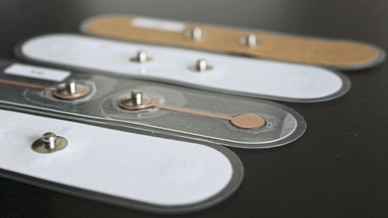
:quality(80)/p7i.vogel.de/wcms/22/82/22826566c11220ed61efac5982fb94a2/0132896083v1.jpeg "Electrodes made from paper and copper paste deliver comparable signal quality to the established gold standard. They perform significantly better in all environmental impact analyses. (Image:Screentec)")
:quality(80)/p7i.vogel.de/wcms/c4/9f/c49f5b8173f678f7ef071355b1fbbd7c/yamu-jay-ai-generated-9088888v1.jpeg "As part of a strategic partnership, Siemens and Reinhausen are advancing the future of energy supply solutions for AI data centers. (Symbol image) (Source: pixabay / AI-generated)")
:quality(80)/p7i.vogel.de/wcms/28/20/28204a4592a69a8682bfbf9a8f7e1dc2/0132846993v1.jpeg "The health status of a lithium-ion battery changes with increasing aging. AI models can utilize characteristic changes in the charge and voltage curves to estimate the state of health. (Image:freely licensed)")
:quality(80)/p7i.vogel.de/wcms/90/dc/90dc332e30a3e4bd3ff77646ed0633b7/0132833369v1.jpeg "Through a compromised repository of the widely used open-source tool LiteLLM, attackers were able to capture several terabytes of data and login credentials. Security company CloudSEK concludes, after analyzing the data, that the attack conducted in March of this year affected more than 2,000 companies, including major players like Microsoft, Nvidia, AWS, and Deutsche Bahn. (Image:freely licensed)")
:fill(fff,0)/p7i.vogel.de/companies/69/88/69882c428938e/tmts2026-ticec-banner-en-2000px.png "tmts2026-ticec-banner-en-2000px (https://www.tmts.tw/en)")
Date: 08.12.2025
Naturally, we always handle your personal data responsibly. Any personal data we receive from you is processed in accordance with applicable data protection legislation. For detailed information please see our privacy policy.
Consent to the use of data for promotional purposes
I hereby consent to Vogel Communications Group GmbH & Co. KG, Max-Planck-Str. 7-9, 97082 Würzburg including any affiliated companies according to §§ 15 et seq. AktG (hereafter: Vogel Communications Group) using my e-mail address to send editorial newsletters. A list of all affiliated companies can be found here
Newsletter content may include all products and services of any companies mentioned above, including for example specialist journals and books, events and fairs as well as event-related products and services, print and digital media offers and services such as additional (editorial) newsletters, raffles, lead campaigns, market research both online and offline, specialist webportals and e-learning offers. In case my personal telephone number has also been collected, it may be used for offers of aforementioned products, for services of the companies mentioned above, and market research purposes.
Additionally, my consent also includes the processing of my email address and telephone number for data matching for marketing purposes with select advertising partners such as LinkedIn, Google, and Meta. For this, Vogel Communications Group may transmit said data in hashed form to the advertising partners who then use said data to determine whether I am also a member of the mentioned advertising partner portals. Vogel Communications Group uses this feature for the purposes of re-targeting (up-selling, cross-selling, and customer loyalty), generating so-called look-alike audiences for acquisition of new customers, and as basis for exclusion for on-going advertising campaigns. Further information can be found in section “data matching for marketing purposes”.
In case I access protected data on Internet portals of Vogel Communications Group including any affiliated companies according to §§ 15 et seq. AktG, I need to provide further data in order to register for the access to such content. In return for this free access to editorial content, my data may be used in accordance with this consent for the purposes stated here. This does not apply to data matching for marketing purposes.
Right of revocation
I understand that I can revoke my consent at will. My revocation does not change the lawfulness of data processing that was conducted based on my consent leading up to my revocation. One option to declare my revocation is to use the contact form found at https://contact.vogel.de. In case I no longer wish to receive certain newsletters, I have subscribed to, I can also click on the unsubscribe link included at the end of a newsletter. Further information regarding my right of revocation and the implementation of it as well as the consequences of my revocation can be found in the data protection declaration, section editorial newsletter.
:quality(80)/p7i.vogel.de/wcms/68/68/68680d52f88c9e11cf09745e7b532dcf/0128050072v1.jpeg "NFC product passports are designed to help consumers use items for longer instead of disposing of them prematurely. (Image: ©Thirawat - stock.adobe.com)")
:quality(80)/p7i.vogel.de/wcms/de/75/de750a367b39ed3167210c6941b067b6/0129059153v1.jpeg "Figure 1: Preparation for the Cyber Resilience Act. By December 2027, device manufacturers must have implemented a series of mandatory measures. (Image:Microchip)")