


:quality(80)/p7i.vogel.de/wcms/88/91/88915656ec26bd5f6e79ce0e523dd33b/0131576263v1.jpeg "Dr. Volker Nilles is CEO of Arburg GmbH + Co KG. In this role, he leads the six-member executive team and, since the beginning of the year, has been responsible for steering the course of the manufacturer of injection molding machines and digital systems for plastics processing. The family-owned company, based in Loßburg, employs approximately 3,400 people worldwide and has a history spanning more than 100 years. (Image: Arburg GmbH + Co. KG)")
:quality(80)/p7i.vogel.de/wcms/81/d4/81d47ab5407c961b55233009313ac9d2/0133075510v1.jpeg "Small, but designed for demanding applications: KSK demonstrates that the diameter of ball screws says nothing about their load-carrying capacity. (Image:Arkero)")
:quality(80)/p7i.vogel.de/wcms/6b/80/6b80bac3b1b33a0e3bc17849bef4ba59/0133171618v1.jpeg "With its portal solution for the MAK 4 Evolution UD swivel-bending machine, Schröder enables the fully automated production of sheet-metal enclosures. (Image:Schröder Group)")
:quality(80)/p7i.vogel.de/wcms/a0/1d/a01ddede6a787a4844122c2f42cfbce9/0133067101v1.jpeg "In solar module manufacturing, lasers are used for tasks such as patterning, drilling, and cutting delicate layers. Precise energy delivery is crucial to avoid damaging adjacent areas. (Image:Dall-E / AI-generated)")
:quality(80)/p7i.vogel.de/wcms/13/2d/132df0ce425eb46f046ffe1065912b19/699704-he-xiaopeng-und-iron-36d230-original-1788864307v1.png "He Xiaopeng hangs an employee ID badge around the neck of the humanoid \"IRON,\" as part of the team. (Source: Xpeng)")
:quality(80)/p7i.vogel.de/wcms/cc/80/cc8031ca517f9ff98cec245efa899b25/0133211591v1.jpeg "The two CEOs of the companies: Max Mauri of Seco and David Reger of Neura. (Image:Neura Robotics)")
:quality(80)/p7i.vogel.de/wcms/ae/eb/aeeb20bb1bf0e6226c35d50b11551a89/0133237319v1.jpeg "At ArcelorMittal Bremen, steel coils are cut to size using blades, a process that takes place at high speed. This makes it difficult to ensure the quality of both the product and the blades. However, TS Sensors and Selmatec have now developed a real-time system ... (Image:AT Sensors)")
:quality(80)/p7i.vogel.de/wcms/ee/de/eedeb235bb6ee164059ea34e6bea795f/0132989868v1.jpeg "From a small Irish bakery to a major manufacturer with expansion plans: Processes can only be scaled through real-time data transparency. (Image:West-Bake)")
:quality(80)/p7i.vogel.de/wcms/6e/1a/6e1ac5a0f1f7b4e9d0b42d34ab3fc47b/geda-sh250w-1v1.jpeg "According to the manufacturer, the battery-powered lift for wind turbines sets new standards in safety, availability, and efficiency. (Source: Geda GmbH)")
:quality(80)/p7i.vogel.de/wcms/45/20/45208dbb0868aa49d32ded081173ebdb/siemens-sarla-aviation-01v1.jpeg "To ensure that data does not remain isolated in individual departments or systems, three companies are leveraging the Digital Thread with Siemens solutions. (Source: Sarla Aviation)")
:quality(80)/p7i.vogel.de/wcms/92/e9/92e9f029ef416e02b6f0b772b39c30df/limbitless-stratasys-zacharyv1.jpeg "The renewed focus of the expanded partnership between Stratasys and Limbitless is on sustainability, education, and improved access to 3D-printed prosthetics. (Source: Stratasys)")
:quality(80)/p7i.vogel.de/wcms/01/f1/01f16ebdc19b9cbde5bc1a7f421f9174/csm-a264340-web-1440-d0360d8de9v1.webp "At the 2026 Dutch Grand Prix in late August, two filtration systems developed by TU Berlin were used in top-level motorsports for the first time. (Source: Audi Revolut F1 Team)")
:quality(80)/p7i.vogel.de/wcms/00/ad/00adb77750d3b28827e3739e6812f803/manuel-mengelkoch-director-sales-operations-volvo-trucks-2v1.jpeg "Manuel Mengelkoch is Director of Sales Operations at Volvo Trucks Germany. (Source: Volvo Trucks)")
:quality(80)/p7i.vogel.de/wcms/9e/fa/9efac6ebae50b1cad8fdb76e3877e692/ex60-global-media-drive-in-barcelona-kleinv1.jpeg "In 2025, electric cars will cost about one-third less to operate in Europe than vehicles with internal combustion engines. (Source: Volvo)")
:quality(80)/p7i.vogel.de/wcms/f3/d5/f3d5d5a330ab5425c90e6a37d23627ba/jag-f-type-heritage60edition-21my-091220-09v1.jpeg "Jaguar Land Rover is cutting 4,000 jobs. (Source: Jaguar Land Rover)")
:quality(80)/p7i.vogel.de/wcms/9e/6e/9e6eadbb44711dca055482f29b651ca9/0133192930v1.jpeg "At Automechanika, Stellantis' SUSTAINera business unit is introducing a remanufactured NOx sensor. (Image:Stellantis)")
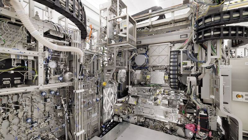
:quality(80)/p7i.vogel.de/wcms/c4/b5/c4b5badd67b0037f23c1d69806a13d16/0133216860v1.jpeg "Fascinating Technology: ASML's NXE3800E EUV machine. (Image:ASML)")
:quality(80)/p7i.vogel.de/wcms/7c/57/7c5719c462b2973564651ca5e472bb58/0133230109v1.jpeg "Prototype of the Diamond Spin Quantum Computer: Users can operate it using the Fujitsu Hybrid Quantum Computing Platform, even without any additional specialized knowledge. (Image:Fujitsu)")
:quality(80)/p7i.vogel.de/wcms/87/96/879685114467b0fe5a43f25923787762/set-explosion-2000pxv1.jpeg "Not explosive, but safe: The new KDS-Rail Fire Safety Kit. (Source: Conta-Clip)")
:quality(80)/p7i.vogel.de/wcms/a4/4e/a44e89f5d47d037ca5d0c870b8dabc65/0133203720v1.jpeg "Transparent DC charging connector from Lapp featuring the vSECC.InPlug communication controller board from Vector (Image:Vector Informatics)")
:fill(fff,0)/p7i.vogel.de/companies/69/de/69de1b7403b0d/simtos-logo.jpeg "simtos-logo (SIMTOS)")
:quality(80)/p7i.vogel.de/wcms/04/a5/04a55af7c725abd266c1afc3a4f494a8/0131668052v1.jpeg "TSMC CEO C.C. Wei sees a chip shortage on the global market for years to come, driven by the high demands of the ongoing AI boom. However, the company intends to keep prices stable despite fully utilized capacities. (Image:TMSC)")
Date: 08.12.2025
Naturally, we always handle your personal data responsibly. Any personal data we receive from you is processed in accordance with applicable data protection legislation. For detailed information please see our privacy policy.
Consent to the use of data for promotional purposes
I hereby consent to Vogel Communications Group GmbH & Co. KG, Max-Planck-Str. 7-9, 97082 Würzburg including any affiliated companies according to §§ 15 et seq. AktG (hereafter: Vogel Communications Group) using my e-mail address to send editorial newsletters. A list of all affiliated companies can be found here
Newsletter content may include all products and services of any companies mentioned above, including for example specialist journals and books, events and fairs as well as event-related products and services, print and digital media offers and services such as additional (editorial) newsletters, raffles, lead campaigns, market research both online and offline, specialist webportals and e-learning offers. In case my personal telephone number has also been collected, it may be used for offers of aforementioned products, for services of the companies mentioned above, and market research purposes.
Additionally, my consent also includes the processing of my email address and telephone number for data matching for marketing purposes with select advertising partners such as LinkedIn, Google, and Meta. For this, Vogel Communications Group may transmit said data in hashed form to the advertising partners who then use said data to determine whether I am also a member of the mentioned advertising partner portals. Vogel Communications Group uses this feature for the purposes of re-targeting (up-selling, cross-selling, and customer loyalty), generating so-called look-alike audiences for acquisition of new customers, and as basis for exclusion for on-going advertising campaigns. Further information can be found in section “data matching for marketing purposes”.
In case I access protected data on Internet portals of Vogel Communications Group including any affiliated companies according to §§ 15 et seq. AktG, I need to provide further data in order to register for the access to such content. In return for this free access to editorial content, my data may be used in accordance with this consent for the purposes stated here. This does not apply to data matching for marketing purposes.
Right of revocation
I understand that I can revoke my consent at will. My revocation does not change the lawfulness of data processing that was conducted based on my consent leading up to my revocation. One option to declare my revocation is to use the contact form found at https://contact.vogel.de. In case I no longer wish to receive certain newsletters, I have subscribed to, I can also click on the unsubscribe link included at the end of a newsletter. Further information regarding my right of revocation and the implementation of it as well as the consequences of my revocation can be found in the data protection declaration, section editorial newsletter.
:quality(80)/p7i.vogel.de/wcms/84/cc/84cc506003388ecffaab464677c7afa6/0129843694v1.jpeg "Launched last year, ASML's TWINSCAN XT:260 is an i-line scanner with a throughput of 270 wafers per hour. With a focus on the increased demands of AI chips, ASML wants to shift its focus away from pure front-end tools for chip production in the next ten to fifteen years with packaging and bonding technologies. (Image:ASML)")
:quality(80)/p7i.vogel.de/wcms/61/9d/619d8849d4790159707bd796d17bbebd/0128679771v1.jpeg "The EXE:5000 from ASML. Version EXE:5200B has brought High-NA EUV lithography technology to production maturity. (Image:ASML)")