Lasers perform a wide range of tasks in the manufacture of crystalline silicon and thin-film modules—from drilling and patterning to welding electrical connections. Selective laser processes are also opening up new possibilities in recycling.
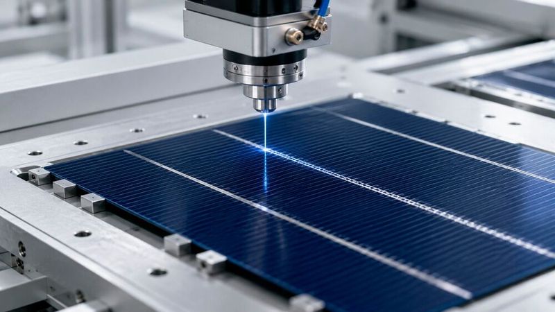
In solar module manufacturing, lasers are used for tasks such as patterning, drilling, and cutting delicate layers. Precise energy delivery is crucial to avoid damaging adjacent areas.
(Image: Dall-E / AI-generated)
Lukas Remshagen is a Key Account Manager at Laserax.
The global photovoltaic market is growing at a remarkable rate. In 2023, 449 GW of capacity was installed. In 2024, this figure rose by 33 percent to 597 GW. Solar Power Europe predicts that 1 TW per year is a realistic goal starting in 2030.
China, the U.S., India, Germany, and Brazil saw the largest growth in installations. In the U.S., two-thirds of all new electricity-generating capacity to solar energy. This is partly due to increased domestic production, which rose by 190 percent compared to 2023.
Different Manufacturing Approaches for Two Types of Solar Modules
There are two main types of solar modules, each of which uses slightly different laser manufacturing techniques:
1. Crystalline Silicon Solar Cells
2. Laser Applications for Thin-Film Solar Modules
Crystalline silicon modules are the most widely used and account for about 95 percent of the global market. Production is concentrated primarily in China, where economies of scale have drastically reduced costs. These modules consist of individual silicon wafers that must be precisely joined together to form functional modules.
In contrast, thin-film modules account for only 5 percent of the global market. In the U.S., however, according to the U.S. Department of Energy, thin-film technology 17 percent of all installations and 25 percent of installations by electric utilities. Thin-film technologies such as CIGS (copper-indium-gallium-selenide) and CdTe (cadmium telluride) are produced by depositing semiconductor layers directly onto glass substrates.
These differences in structure necessitate different methods of laser processing. While the manufacturing process for crystalline silicon focuses on the preparation of individual cells and their interconnection, thin-film production requires the precise creation of structures within the layers to produce cells connected in series on a single substrate.
Laser Applications in the Manufacture of Crystalline Silicon Modules
Lasers are used at several stages in the manufacturing of crystalline silicon modules. This always requires precise control of the parameters to prevent damage to the sensitive silicon substrates.
Laser edge isolation: Laser edge isolation removes conductive layers from the wafer edges after doping and texturing. This process prevents leakage currents that could reduce efficiency and lead to safety risks. The challenge lies in removing conductive materials from the thin silicon wafers without compromising their structural integrity.
Laser drilling for PERC cells: Laser drilling is one of the most technically challenging applications in the manufacture of crystalline silicon modules. PERC (Passivated Emitter and Rear Cell) technology requires thousands of microscopic contact holes in the rear passivation layer. These holes typically have a diameter of 20–30 micrometers (0.0008–0.0012 inches) and must completely penetrate the passivation layer without damaging the underlying silicon substrate. This requires exceptional precision. Process windows measured in nanoseconds determine whether the holes establish the correct electrical contact or cause defects.
Laser Scribing/Ablation: Scribing and ablation are used to fine-tune cell dimensions and create isolation trenches in the micrometer range by removing layers of materials such as silicon, transparent conductive oxides, or metallization layers. The selectivity of the laser wavelengths makes it possible to process specific materials while leaving the adjacent layers intact.
Laser Welding of Connections: In the final step, lasers with precisely controlled wavelengths join the copper wires and busbars. This process creates strong, low-resistance electrical connections without generating excessive heat that could damage the silicon cells.
Laser Applications in the Manufacturing of Thin-Film Modules
The manufacture of thin-film modules demonstrates laser technology's ability to create complex electrical architectures through integrated processing.
The three-step engraving sequence relies on precise process control. Each laser operation builds on the previous steps to create a functional photovoltaic module.
P1 Scribing: In the first step, structures are created in the back-side contact layer immediately after application, thereby laying the foundation for delineating the individual cells. The laser must completely remove the metallic contact on the back side without damaging the underlying glass substrate. Line widths can range from 50 to 100 micrometers (0.002 to 0.004 inches), and minimizing dead zones is a critical performance factor.
P2 Slicing: After the absorber layer is deposited, the individual cells are isolated by removing the semiconductor material down to the back-side contact layer. This step requires a high degree of precision, as the laser must stop exactly at the interface between the absorber layer and the back-side contact layer. If the groove is cut too deep, it would damage the back-side contact layer. If it is not cut deep enough, short circuits will occur between adjacent cells.
P3 grooving: In the final step, the front contact layer—which typically consists of a transparent, conductive oxide—is patterned using lasers. This connects the front contact of one cell to the rear contact of the adjacent cell, establishing the connection required for operation.
Edge insulation: Next, the active layers at the outer edge are removed using lasers, which is necessary to prevent leakage currents. This process is particularly important for thin-film modules, where edge insulation is the most important mechanism for preventing ground faults due to their monolithic architecture.
Lasers in Solar Panel Recycling
As the number of end-of-life solar modules grows, their recycling is becoming increasingly important. Laser-based methods are being explored—and in some cases are already being used—to selectively separate different material layers from one another. Their main advantage lies in their non-contact and selective processing. However, a fully laser-based recycling process has not yet been economically established in all applications.
Delamination: Lasers can locally heat or ablate encapsulation materials such as ethylene-vinyl acetate (EVA) or polyolefin elastomers (POE). This allows glass and silicon components to be separated from one another without subjecting the underlying materials to significant mechanical stress. Depending on the module design, this can enable a more precise separation than purely mechanical methods.
Contact Removal: Laser ablation can be used to selectively remove metal contacts and coatings from crystalline silicon wafers. The goal is to cause as little damage as possible to the underlying silicon, thereby facilitating further material recycling.
Glass Cleaning: Even residual polymer and adhesive residues can be removed from glass substrates using laser techniques. This allows the glass to be prepared for further recycling or reuse processes without having to rely exclusively on chemical or abrasive cleaning methods.
Recycling of thin-film modules: In thin-film modules, lasers can selectively ablate individual semiconductor layers, such as cadmium telluride or CIGS, while the glass substrate remains largely intact. Such processes could help in the future to recover valuable materials in a more targeted manner and reduce the use of chemical separation processes.
The Key Benefits of Laser Technology in Solar Manufacturing
Laser technology plays a key role in every phase of solar production, helping to streamline manufacturing and improve yields. Here are just a few of the benefits.
Precision and Efficiency: Lasers are highly precise and enable high-density interconnection patterns and effective use of the active area. Laser texturing can create microscopic surface structures that reduce reflection and increase light absorption. This enables higher power output. These surface modifications can improve cell efficiency.
A recent study shows efficiency gains of up to 0.22 percent. That may not seem like much, but given the global sales volume of solar modules, it really adds up.
Improved Light Absorption: Laser-generated surface structures improve photon absorption in solar cells, particularly in thin-film applications, since the length of the absorption paths is limited. This also reduces energy loss by isolating the current paths.
Scalability: Non-contact processing enables high-throughput production without concerns about mechanical wear or tool changes. This speeds up production cycles and avoids frequent interruptions for maintenance or replacement.
Consistent results: The precisely controlled energy input remains constant, which improves quality and ensures consistent results even for large print runs.
Promoting Growth in the Solar Industry
Laser processes perform a variety of tasks in the manufacturing and, increasingly, the recycling of solar modules. Their strengths lie in particular in precise, non-contact, and selective processing. At the same time, new cell architectures and materials are placing greater demands on process control. Lasers can enable targeted energy input without unnecessarily stressing adjacent structures.
Date: 08.12.2025
Naturally, we always handle your personal data responsibly. Any personal data we receive from you is processed in accordance with applicable data protection legislation. For detailed information please see our privacy policy.
Consent to the use of data for promotional purposes
I hereby consent to Vogel Communications Group GmbH & Co. KG, Max-Planck-Str. 7-9, 97082 Würzburg including any affiliated companies according to §§ 15 et seq. AktG (hereafter: Vogel Communications Group) using my e-mail address to send editorial newsletters. A list of all affiliated companies can be found here
Newsletter content may include all products and services of any companies mentioned above, including for example specialist journals and books, events and fairs as well as event-related products and services, print and digital media offers and services such as additional (editorial) newsletters, raffles, lead campaigns, market research both online and offline, specialist webportals and e-learning offers. In case my personal telephone number has also been collected, it may be used for offers of aforementioned products, for services of the companies mentioned above, and market research purposes.
Additionally, my consent also includes the processing of my email address and telephone number for data matching for marketing purposes with select advertising partners such as LinkedIn, Google, and Meta. For this, Vogel Communications Group may transmit said data in hashed form to the advertising partners who then use said data to determine whether I am also a member of the mentioned advertising partner portals. Vogel Communications Group uses this feature for the purposes of re-targeting (up-selling, cross-selling, and customer loyalty), generating so-called look-alike audiences for acquisition of new customers, and as basis for exclusion for on-going advertising campaigns. Further information can be found in section “data matching for marketing purposes”.
In case I access protected data on Internet portals of Vogel Communications Group including any affiliated companies according to §§ 15 et seq. AktG, I need to provide further data in order to register for the access to such content. In return for this free access to editorial content, my data may be used in accordance with this consent for the purposes stated here. This does not apply to data matching for marketing purposes.
Right of revocation
I understand that I can revoke my consent at will. My revocation does not change the lawfulness of data processing that was conducted based on my consent leading up to my revocation. One option to declare my revocation is to use the contact form found at https://contact.vogel.de. In case I no longer wish to receive certain newsletters, I have subscribed to, I can also click on the unsubscribe link included at the end of a newsletter. Further information regarding my right of revocation and the implementation of it as well as the consequences of my revocation can be found in the data protection declaration, section editorial newsletter.



:quality(80)/p7i.vogel.de/wcms/9e/23/9e23111e49d73012e9e3b7c69428ad5c/0134019347v1.jpeg "The Dominant VA45 high-helix tap from Bass, made of lead-free brass. The long chips, which result from the absence of lead, are clearly visible. (Image:Bass, Inc.)")
:quality(80)/p7i.vogel.de/wcms/1d/09/1d0999956ef87709b72ab1d0402ba207/csf-minis-gruppe-final-01-outputv1.jpeg "Since mid-2026, Harmonic Drive has been offering its CSF Mini gearheads in size 7 as well, in six variants designed for different installation scenarios. (Source: Harmonic Drive)")
:quality(80)/p7i.vogel.de/wcms/ab/08/ab08675922c3a7edea45128248b45b00/0133857009v1.jpeg "In the aerospace industry—one of the most demanding sectors of all—the Shanghai-based company TOPNC has already made a name for itself. (Image:TOPNC)")
:quality(80)/p7i.vogel.de/wcms/ff/48/ff48b1154746e79128935f28bd73ba0e/0113143253v1.jpeg "In our China Market Insider, we regularly provide you with relevant information straight from China. (Image:© Eisenhans - stock.adobe.com)")
:quality(80)/p7i.vogel.de/wcms/ca/24/ca24d741a2fd714fa14d2a3e9db1c904/image1v1.jpeg "With 117,500 units sold, transportation and logistics will remain the leading application area for service robotics in 2025 as well. (Image:Innok Robotics)")
:quality(80)/p7i.vogel.de/wcms/b7/95/b795d5fb82459f8a526e880f0698dffa/1-maxon-mind-covershot-landscapev1.jpeg "Claude Jaquemet demonstrates the Maxon Mind demo system. (Source: Maxon)")
:quality(80)/p7i.vogel.de/wcms/be/66/be661616d5250d4c3814a25688f3904b/0133917202v1.jpeg "Neuron AI combines 3D vision, touch, hearing, proprioception, and language—along with memory—into a Perception-Language-Action (PLA) model. Robots can grasp objects they cannot see. (Image:Neura)")
:quality(80)/p7i.vogel.de/wcms/c7/12/c712b688dba2262fa3906e3a4c1d2f7d/humanoide-robotikv1.jpeg "“Find a job that the humanoid can actually do, and understand your processes”—that’s the advice robotics expert Sebastian Prinz gives companies so they can benefit from the technology in the long term. (Source: Fraunhofer IEM / Janosch Gruschczyk)")
:quality(80)/p7i.vogel.de/wcms/51/b8/51b8e08d2105fdd9952aff385f154192/graphic-2-adma1v1.png "The new surface hardening process enhances the performance of corrosion-resistant alloys by improving their tribological and mechanical surface properties, while preserving the properties of the base material. (Source: Bodycote)")
:quality(80)/p7i.vogel.de/wcms/96/ef/96effc239916cb7e0f396ab75627b8c0/image-space-testingv1.jpeg "Two scientists in front of a vacuum chamber used for testing: As technical instruments for spaceflight become more sensitive, the test facilities are becoming a critical system. (Source: Busch Group)")
:quality(80)/p7i.vogel.de/wcms/5a/12/5a1294a38a634f839f542c0055024d7a/jie-yin-feather-star-header-1500v1.jpeg "Underwater Acrobatics: The new soft robot mimics brittle stars—using minimal propulsion technology. (Source: North Carolina State University)")
:quality(80)/p7i.vogel.de/wcms/96/89/9689197f666e4aa9bc4a1f395c25d3ef/0133739635v1.jpeg "The 2026 Nobel Prize in Medicine laureates: Karl Deisseroth, Peter Hegemann, and Georg Nagel. (Image:Nobel Prize Outreach)")
:quality(80)/p7i.vogel.de/wcms/fe/f7/fef766ae8b8310ca6dd0852208923e4e/hendrik-malinowski-coo-01v1.png "Hendrik Malinowski Takes on New Role as CCO of BUGATTI RIMAC (Source: Bugatti)")
:quality(80)/p7i.vogel.de/wcms/d9/5f/d95fd82eb5368ce77a8bc9de3a085376/yoshihiro-nakatav1.jpeg "“We are a European manufacturer”: Yoshihiro Nakata, CEO of Toyota Motor Europe, at the corporate briefing in Brussels. (Image:Toyota)")
:quality(80)/p7i.vogel.de/wcms/e3/0b/e30b87c9b7a6c41b7e7336f34f0a8214/0133970831v1.jpeg "Tesla's planned expansion of vehicle and battery production capacity in Grünheide, near Berlin, appears to be gaining momentum, according to a recent announcement by the U.S. electric car manufacturer ... (Image: AI-generated)")
:quality(80)/p7i.vogel.de/wcms/23/5f/235fa4afabc57699636224d17e106b4b/kraemer-p2p-display-technologyv1.png "The cockpit display system from Krämer Automotive Systems shows driving-related information, infotainment, and vehicle functions. (Source: Krämer Automotive)")
:quality(80)/p7i.vogel.de/wcms/8b/35/8b35660420abba32fb891a4c5cc42fbd/0134018092v1.jpeg "Long-range UVC LED with lens and reflector: Close-up of a square LED with a transparent, dome-shaped lens on a dark base plate. The hermetically sealed housing ensures greater reliability and durability under demanding environmental conditions. (Image:FBH_Schurian)")
:quality(80)/p7i.vogel.de/wcms/a4/1c/a41cd52e0a26e5173bd4e1f834d4f7f4/0134025034v1.jpeg "As chips become more complex, the demands on semiconductor testing increase. Teradyne and FormFactor plan to combine their technologies for future applications. (Image:freely licensed)")
:quality(80)/p7i.vogel.de/wcms/7b/64/7b64e9fe595b88d2b01ed79e0f2baf94/pm-weidm-ller-elatec-substation-line-switchv1.jpeg "Caption: The Substation Line managed switches can accommodate up to three HSR/PRP modules. (Image:Weidmüller)")
:quality(80)/p7i.vogel.de/wcms/b3/bf/b3bf55a31510b319bb473f73aa205477/0133987448v1.jpeg "In court, Qualcomm achieved a partial victory in its legal dispute with Arm, but was awarded only a symbolic $2 in damages—for now. (Image:Dall-E / AI-generated)")
:fill(fff,0)/images.vogel.de/vogelonline/companyimg/76800/76895/65.jpg "FAULHABER_120mm.jpg ()")
:quality(80)/p7i.vogel.de/wcms/01/71/01719553413411b4e0d931277934f866/0131873657v1.jpeg "0131873657v1 (Image: Imec)")
:quality(80)/p7i.vogel.de/wcms/3d/1b/3d1bb141472f63720c90957948d7a7cf/0128578467v1.jpeg "Johanna Byloff analyzes the samples at the coating machine of the Empa spin-off Swiss Cluster. (Image:Empa)")