The accelerating shift toward software-defined products is redefining the industry's expectations for electronics and semiconductor components. In modern vehicles, for example, many key functions are now enabled by electromechanical systems, a centralized computing architecture, and software that evolves over time.
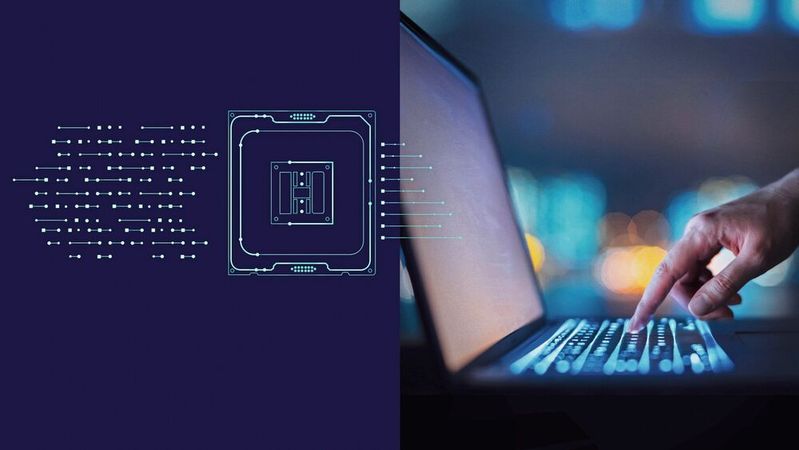
Demand for electronics and semiconductor products is expected to continue growing, prompting manufacturers to innovate and ramp up production while overcoming challenges.
(Image: Siemens)
This transformation ultimately depends on silicon. Software applications, industrial AI, and increasingly intelligent systems require powerful, efficient, and reliable computing hardware. Industry forecasts predict that the electronics and semiconductor industry could reach a total market value of $1.6 trillion by 2030. However, as demand continues to rise, development cycles are shrinking, energy constraints are increasing, talent is in short supply, and resilience in the face of geopolitical and supply chain disruptions is becoming increasingly critical.
To cope with this pressure, semiconductor companies need development approaches tailored to a software-defined, silicon-based, and AI-powered future. As chip designs become exponentially more complex and advanced packaging technologies evolve, the economics of innovation mean that traditional, siloed approaches to design, manufacturing, and operations can no longer keep pace.
A comprehensive Digital Twin strategy that covers the entire semiconductor lifecycle—from design planning through factory construction, manufacturing, buildings, infrastructure, and operations—provides the foundation for faster and more confident decision-making. By integrating product, production, and performance data, semiconductor designers and manufacturers can improve lifecycle continuity, accelerate time-to-value, and lay the digital foundation required for industrial AI.
Connecting the Semiconductor Life Cycle Through Digitalization
Design engineers in the semiconductor industry have relied on digital models for decades because chip development is complex. The next step is to extend this capability beyond design to include manufacturing, production operations, and performance, thereby creating a seamless connection between the digital and physical worlds throughout the entire semiconductor lifecycle.
Deeper integration between design, manufacturing, and operations will help semiconductor companies more efficiently manage the growing complexity and technical challenges involved in developing and manufacturing the next generation of chips. Shrinking process nodes are only part of the challenge. Advanced packaging techniques such as 3D-ICs introduce new design and manufacturing dependencies, while software workloads increasingly dictate chip requirements. Semiconductor companies therefore need closer integration across different disciplines so that silicon performance, software behavior, energy efficiency, and manufacturability can be jointly evaluated earlier in the process.
It is crucial that decisions made during the design phase determine the final manufacturing results. Design engineers must consider system performance, energy efficiency, chip reuse, and circularity from the very beginning. A comprehensive digital twin approach helps teams make critical decisions earlier, explore trade-offs virtually, and optimize the product, production, and performance before committing resources in the real world—fundamentally transforming how semiconductor companies approach development.
An Interconnected Database Lays the Foundation
Data fragmentation remains one of the biggest hurdles to digital transformation. Industry research by Tech-Clarity shows that 60 percent of semiconductor companies use six or more separate systems to store and access product lifecycle management data. This fragmentation slows down collaboration and creates invisible barriers to innovation and efficiency, with teams in design, manufacturing, and operations too often working with incomplete or inconsistent information.
The challenge is becoming increasingly urgent as companies adopt industrial AI. AI can only deliver reliable industrial results if it is based on high-quality, contextualized, and trustworthy data. Without a unified data backbone, organizations risk investing in advanced capabilities that are difficult to scale or validate in high-risk environments.
Disconnected data systems hinder innovation and limit the effectiveness of advanced technologies such as artificial intelligence.
(Image: gorodenkoff/iStock)
A successful digital transformation therefore begins with the continuity of lifecycle data. A connected data backbone links previously disconnected systems, creates a shared context, and enables companies to apply the comprehensive digital twin and industrial AI across the entire silicon lifecycle. This is not simply an IT exercise; it lays the foundation for faster decision-making, more resilient operations, and continuous optimization.
Date: 08.12.2025
Naturally, we always handle your personal data responsibly. Any personal data we receive from you is processed in accordance with applicable data protection legislation. For detailed information please see our privacy policy.
Consent to the use of data for promotional purposes
I hereby consent to Vogel Communications Group GmbH & Co. KG, Max-Planck-Str. 7-9, 97082 Würzburg including any affiliated companies according to §§ 15 et seq. AktG (hereafter: Vogel Communications Group) using my e-mail address to send editorial newsletters. A list of all affiliated companies can be found here
Newsletter content may include all products and services of any companies mentioned above, including for example specialist journals and books, events and fairs as well as event-related products and services, print and digital media offers and services such as additional (editorial) newsletters, raffles, lead campaigns, market research both online and offline, specialist webportals and e-learning offers. In case my personal telephone number has also been collected, it may be used for offers of aforementioned products, for services of the companies mentioned above, and market research purposes.
Additionally, my consent also includes the processing of my email address and telephone number for data matching for marketing purposes with select advertising partners such as LinkedIn, Google, and Meta. For this, Vogel Communications Group may transmit said data in hashed form to the advertising partners who then use said data to determine whether I am also a member of the mentioned advertising partner portals. Vogel Communications Group uses this feature for the purposes of re-targeting (up-selling, cross-selling, and customer loyalty), generating so-called look-alike audiences for acquisition of new customers, and as basis for exclusion for on-going advertising campaigns. Further information can be found in section “data matching for marketing purposes”.
In case I access protected data on Internet portals of Vogel Communications Group including any affiliated companies according to §§ 15 et seq. AktG, I need to provide further data in order to register for the access to such content. In return for this free access to editorial content, my data may be used in accordance with this consent for the purposes stated here. This does not apply to data matching for marketing purposes.
Right of revocation
I understand that I can revoke my consent at will. My revocation does not change the lawfulness of data processing that was conducted based on my consent leading up to my revocation. One option to declare my revocation is to use the contact form found at https://contact.vogel.de. In case I no longer wish to receive certain newsletters, I have subscribed to, I can also click on the unsubscribe link included at the end of a newsletter. Further information regarding my right of revocation and the implementation of it as well as the consequences of my revocation can be found in the data protection declaration, section editorial newsletter.
How Digital Twins Speed Up the Construction of Fabs
Fab Construction is a clear example of how digitalization can reduce risks and increase value. Traditional manufacturing projects involve sequential phases with limited opportunities to test operational assumptions before billions in capital expenditures are committed. A digital-native approach changes this sequence by creating complete virtual models before construction begins. Engineers can simulate entire facilities, test material flows, optimize equipment placement, validate staffing assumptions, and examine environmental controls in a risk-free digital environment.
With the Digital Twin, semiconductor manufacturers can virtually plan and test production optimizations—from identifying bottlenecks and improving cleanroom layouts to validating equipment monitoring and control systems. The result is a shorter ramp-up time and lower risk between project completion and mass production—a crucial advantage in an industry where time-to-market and yield often determine competitive positioning.
The value extends beyond the construction phase. Digital twin models can be maintained throughout the facility’s entire lifecycle and incorporate operational data to support continuous optimization as products, processes, and market conditions change. For example, the Digital Twin can account for the energy consumption of all systems within a factory, creating an “Energy Twin” that ensures a stable power supply while enabling optimizations to meet cost and sustainability goals.
Ecosystem Collaboration Drives Innovation
Chip designers, foundries, device manufacturers, software teams, and end-application developers all provide key information to create more comprehensive virtual representations of products and processes. Traditional concerns about IP exposure lead to reluctance toward this level of collaboration, but the competitive advantages of secure ecosystem integration are becoming increasingly compelling.
Secure data exchange frameworks enable collaboration while protecting proprietary information. Companies that operate across multiple segments of the value chain can facilitate ecosystem connections and bring together insights from industrial electronics, design tools, manufacturing systems, automation, and end applications. This enables them to learn across industries that face similar challenges in the automotive, aerospace, life sciences, and other sectors.
As products become increasingly software-defined, silicon-enabled, and AI-driven, no single organization can optimize in isolation. Companies that master a secure ecosystem. Collaboration will be better positioned to turn complexity into innovation while maintaining trust, resilience, and control over critical intellectual property.
Securing a Digital Enterprise with a Defense-in-Depth Strategy
The digital transformation in the semiconductor industry must be based on a robust, multi-layered cybersecurity strategy from the very beginning. Semiconductor manufacturing regions and facilities are valuable targets, and increasingly interconnected digital ecosystems are creating new challenges for protecting intellectual property, proprietary technology, and critical infrastructure.
The same connectivity that makes the comprehensive Digital Twin so powerful also expands the attack surface. Digitalization connects systems that were previously isolated, while collaboration within the ecosystem introduces additional points of access. Semiconductor companies must therefore balance openness with strong protection of proprietary data and production systems.
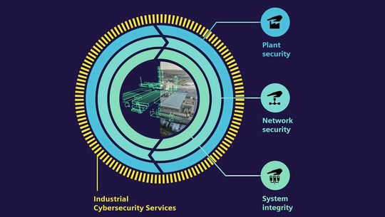
Although digitalization offers enormous benefits, it must be combined with a comprehensive and robust cybersecurity strategy to protect critical systems and intellectual property.
(Image: Siemens)
Industrial cybersecurity strategies such as defense-in-depth address this challenge by creating multiple layers of protection across IT systems, operational technologies, and physical access to facilities. New technologies, particularly AI-powered threat detection, can strengthen this approach by enabling faster responses to emerging risks. Crucially, defense-in-depth strategies prepare for breaches at individual layers and assume that threats will evolve, thereby building resilience into the architecture from the outset.
A Strategic Approach to Digitalization in the Semiconductor Industry
A comprehensive digital twin strategy can enable a fundamental transformation of the way semiconductor companies design, build, manufacture, and operate by connecting the silicon lifecycle from start to finish. The most effective starting point for leaders in the semiconductor industry who want to continue their digital transformation is to achieve measurable gains in existing pain points within the organization, such as yield, time-to-market, energy consumption, technical productivity, or data fragmentation. Early successes can build momentum for a more comprehensive transformation.
From there, companies can scale in line with their business objectives, supported by a unified data backbone, highly accurate simulation capabilities, secure collaboration practices, and cybersecurity integrated from the start. This lays the foundation for industrial AI to create value not as a standalone technology, but as part of a trusted digital enterprise.
Meanwhile, cultural change deserves equal attention. Operations teams must be confident that new approaches will not disrupt production, especially in an industry where downtime incurs enormous costs. Digital simulation and testing environments can help build confidence in new approaches, while investments in training and change management can ensure that the technology rollout leads to sustainable expertise.
The question for semiconductor executives is no longer whether digitalization will transform the industry, but how quickly they can lay the groundwork to implement it on a large scale. With increasing design complexity, power constraints, talent shortages, and ecosystem interdependencies, the comprehensive digital twin offers a practical path to faster decision-making, reduced risk, and continuous optimization. Companies that connect the silicon lifecycle now are better positioned to define the next era of semiconductor innovation.
*Katharina Westrich is Global Vice President of Electronics & Semiconductors at Digital Industries, Siemens AG



:quality(80)/p7i.vogel.de/wcms/6b/80/6b80bac3b1b33a0e3bc17849bef4ba59/0133171618v1.jpeg "With its portal solution for the MAK 4 Evolution UD swivel-bending machine, Schröder enables the fully automated production of sheet-metal enclosures. (Image:Schröder Group)")
:quality(80)/p7i.vogel.de/wcms/a0/1d/a01ddede6a787a4844122c2f42cfbce9/0133067101v1.jpeg "In solar module manufacturing, lasers are used for tasks such as patterning, drilling, and cutting delicate layers. Precise energy delivery is crucial to avoid damaging adjacent areas. (Image:Dall-E / AI-generated)")
:quality(80)/p7i.vogel.de/wcms/6c/98/6c98f4dd0780456713eee6379b3f534f/0132999605v1.jpeg "This specific project involved a similar surgical screw. (Image:KLS Martin)")
:quality(80)/p7i.vogel.de/wcms/e9/90/e9904998fceb618c13613a1660fdfc74/0133135112v1.jpeg "This saw blade lasts up to eight times longer than solid carbide counterparts. This is made possible by an innovative nanocrystalline diamond coating from Oerlikon Balzers, which can also be applied to drill bits and end mills. Here is some information from a project with a user ... (Image:Oerlikon Balzers)")
:quality(80)/p7i.vogel.de/wcms/a0/0c/a00c9b7242fa38414b3281a9cd6dcc39/0133127938v1.jpeg "Demand for electronics and semiconductor products is expected to continue growing, prompting manufacturers to innovate and ramp up production while overcoming challenges. (Image:Siemens)")
:quality(80)/p7i.vogel.de/wcms/13/8a/138a5d6686ba26ad35c8f7593c319359/0133105064v1.jpeg "LAPP uses an automation model to demonstrate how sensors, actuators, cables, and network components reliably transmit data to the cloud. (Image:Lapp)")
:quality(80)/p7i.vogel.de/wcms/88/86/88865040dd97ce19eeb5df398eb9f383/0113143253v1.jpeg "In our China Market Insider, we regularly provide you with relevant information straight from China. (Image:© Eisenhans - stock.adobe.com)")
:quality(80)/p7i.vogel.de/wcms/16/aa/16aa1c99cb3ee4fb784c7e8ed022b395/dlr-eu-1v1.jpeg "AI-based robotics has the potential to develop into an industry in Europe over the next ten to fifteen years that rivals today’s automotive industry in size and importance. Here, you can see how the DLR robot Rollin’ Justin independently performs an everyday task and waters a houseplant. (Image:DLR (CC BY-NC-ND 3.0))")
:quality(80)/p7i.vogel.de/wcms/fd/76/fd76fd67142ded48cfcb2e819bea231b/0133154160v1.jpeg "The pacemaker implant is flexible and conforms to the shape of the brain. This significantly improves comfort. (Image:Fraunhofer IZM)")
:quality(80)/p7i.vogel.de/wcms/8f/82/8f827c555c5af559af362274a9503887/newsimage426603v1.jpeg "The composite material made of epoxy and glass fibers not only protects against flames but is also fully recyclable. (Source: Empa)")
:quality(80)/p7i.vogel.de/wcms/d3/ad/d3ad3f6529839a772acd8741ce83e439/0132390244v1.jpeg "If you make the wrong choice when seeking funding advice, you risk not only wasting time but also missing out on funding opportunities and suffering financial losses. (Image: ©alfa27 - stock.adobe.com)")
:quality(80)/p7i.vogel.de/wcms/94/d5/94d564c8630570efab7bf1afd87afb34/0133150604v1.jpeg "For years, the trend in cars was to have fewer buttons and ever-larger displays. Now, a shift is taking place in China: buttons are making a comeback. (Image:Freely licensed on Pixabay)")
:quality(80)/p7i.vogel.de/wcms/a4/b7/a4b7d453522f2cbb8e89f18b0f48a4e2/0131845932v1.jpeg "Hardly any stress! In the negotiations over VW’s drastic cost-cutting package, agreements have already been reached on several key points. VW CEO Oliver Blume calls this an encouraging sign. Read here to find out what happened on September 3... (Image:Volkswagen)")
:quality(80)/p7i.vogel.de/wcms/d2/36/d236c7089523726327e9d2d3a6c28f9b/0133152555v1.jpeg "To ensure that hydrogen, in addition to electric powertrains for trucks, becomes more widely adopted as an alternative propulsion option, several major companies are now collaborating. Here’s who they are and what exactly this is all about ... (Image:AI-generated)")
:quality(80)/p7i.vogel.de/wcms/3d/bf/3dbf2071d4f39b0a6ae4b1c444fbd4ab/marelli-microchipv1.jpeg "A new technology from Marelli and Microchip transmits graphics and video content from the vehicle's central computer directly to the vehicle's displays. (Source: Marelli / KI-generiert)")
:quality(80)/p7i.vogel.de/wcms/88/62/886275be9b95f912061e9d7e77a3b799/0133171501v1.jpeg "Secure and reliable cloud platforms for businesses have long since become a strategic decision. (Image:Pixabay / Brian Penny / AI-generated)")
:quality(80)/p7i.vogel.de/wcms/0d/da/0dda2dc67d266b0577dd243f8e6321dd/0133153751v1.jpeg "The rising demand for AI infrastructure is having a direct impact on the supply chain and exposing bottlenecks in production. (Image:Broadcom)")
:quality(80)/p7i.vogel.de/wcms/00/71/0071675c8d6f934225a970a9731b905e/0133122313v1.jpeg "From the physical chip to a stable computing environment: The industrial viability of quantum processors is determined by circuit-level performance—not by qubit counts alone. (Image:Gemini / AI-generated)")
:quality(80)/p7i.vogel.de/wcms/38/4d/384de4721339db429ec3a735dd541143/0133124795v1.jpeg "The massive AI industry surrounding Project Stargate is worth billions of dollars, but it also poses significant risks. (Image:Gemini / AI-generated)")
:fill(fff,0)/p7i.vogel.de/companies/69/88/69882c428938e/tmts2026-ticec-banner-en-2000px.png "tmts2026-ticec-banner-en-2000px (https://www.tmts.tw/en)")
:fill(fff,0)/p7i.vogel.de/companies/69/de/69de1b7403b0d/simtos-logo.jpeg "simtos-logo (SIMTOS)")
:quality(80)/p7i.vogel.de/wcms/05/e7/05e7017a2699ef15b513bfd2e18431fb/digitaler-planungszwilling-bildv1.png "The author explains here why the digital twin only becomes a planning tool when it follows a clear decision-making question. (Source: T&O Group/AI-generated)")
:quality(80)/p7i.vogel.de/wcms/78/84/78841963da07ee993f10c21d0e21d5cf/0129237953v1.jpeg "In times of increasingly complex development processes, the digital twin is a key tool for mastering this complexity and implementing products faster. (Image:Siemens)")
:quality(80)/p7i.vogel.de/wcms/f2/b5/f2b56024ad5671dcb99c042462845d9d/0126430991v1.jpeg "The term \"shift-left\" is borrowed from the DevOps cycle and means establishing the testing step as part of software development - and thus no longer relegating it to the end of the development cycle. (Image:Siemens)")