The boundaries between front-end and back-end production are becoming blurred: In addition to EUV, ASML will focus on packaging, bonding and larger exposure fields in the future, announced CTO Marco Pieters in an interview with Reuters. This is in response to the increased demands placed on chips in the AI age.
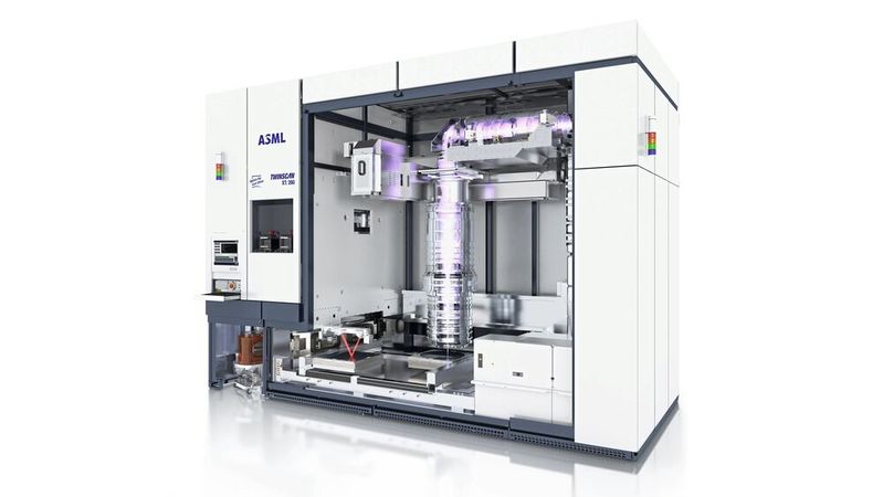
Launched last year, ASML's TWINSCAN XT:260 is an i-line scanner with a throughput of 270 wafers per hour. With a focus on the increased demands of AI chips, ASML wants to shift its focus away from pure front-end tools for chip production in the next ten to fifteen years with packaging and bonding technologies.
(Image: ASML)
With EUV lithography, ASML has a leading technology for the production of advanced chips in small structure sizes. But in the age of AI, it is no longer enough to expose only the finest structures. In an interview with the Reuters news agency, ASML CTO Marco Pieters gave an insight into what kind of tools will be important for the manufacturer of advanced chip manufacturing technologies in the next ten to fifteen years.
From the Front End to Packaging
Advanced packaging is at the heart of this. What was long considered a low-margin back-end process is now becoming a strategic lever for the performance and energy efficiency of modern AI accelerators, says Peters. The growing complexity of chiplet designs is increasingly shifting precision requirements towards packaging and bonding.
Until a few years ago, monolithic dies dominated. Suppliers such as Nvidia and Advanced Micro Devices relied on large, flat chips. Today, heterogeneous systems are created with stacked logic and memory components, connected via the finest through-silicon vias and interposers.
Foundries such as Taiwan Semiconductor Manufacturing Company are driving this development forward with technologies such as CoWoS. Intel is also relying on 3D stacking with Foveros. In both cases, the requirements for overlay accuracy, alignment and process control are increasing significantly.
ASML is therefore examining how existing core competencies from front-end lithography can be transferred to packaging applications. The boundary between front-end and back-end is becoming blurred: optics, wafer handling and high-precision stage systems could also provide competitive advantages in interconnect and bonding processes. The aim is not a broad-based equipment portfolio, but rather targeted expansions with clear technological leverage.
A first step is the XT:260 scanner, which was released at the end of last year and is aimed specifically at advanced memory and AI applications. The system addresses large exposure fields and precise through-silicon alignment and, according to the company, achieves many times the throughput of existing solutions.
Stacking With the Smallest Structure Sizes
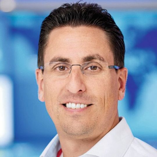
ASML CTO Marco Pieters: ASML has started developing chip manufacturing tools that can help build newer generations of advanced AI processors. "We are currently researching to what extent we can participate or what we can contribute to this part of the business," says Pieters. Packaging and bonding technologies play a special role here.
(Image: ASML)
The metaphor of a skyscraper aptly describes the current development. AI processors are not only growing in size, but also in height. Several specialized dies are being combined vertically and horizontally to increase bandwidth and computing power.
Memory manufacturers such as SK Hynix are developing suitable HBM generations that are closely interlinked with logic chips. As a result, part of the value chain is shifting from the traditional front end to hybrid process chains, where packaging and lithography are moving closer together.
"Accuracy is becoming increasingly important," emphasizes Pieters. With decreasing tolerances in the sub-micrometer range, it is clear that advanced packaging is no longer just a back-end issue, but increasingly affects front-end standards.
Larger Exposure Fields and High-NA
At the same time, ASML is investigating whether the maximum field size can be extended beyond the current "stamp format". Larger dies could map certain AI workloads more efficiently, but come up against the physical and economic limits of exposure.
At the same time, the next EUV generation is being launched. High-NA systems, which initially went to Intel in 2024, are intended to further increase the structure resolution. A third generation is already in the research phase. EUV therefore remains the core of the business, but is being supplemented by new approaches.
Added to this is the increased use of AI in the company's own systems. Faster machines require more complex control algorithms and inline inspection. Here, software-based optimization can further improve throughput and yield.
Date: 08.12.2025
Naturally, we always handle your personal data responsibly. Any personal data we receive from you is processed in accordance with applicable data protection legislation. For detailed information please see our privacy policy.
Consent to the use of data for promotional purposes
I hereby consent to Vogel Communications Group GmbH & Co. KG, Max-Planck-Str. 7-9, 97082 Würzburg including any affiliated companies according to §§ 15 et seq. AktG (hereafter: Vogel Communications Group) using my e-mail address to send editorial newsletters. A list of all affiliated companies can be found here
Newsletter content may include all products and services of any companies mentioned above, including for example specialist journals and books, events and fairs as well as event-related products and services, print and digital media offers and services such as additional (editorial) newsletters, raffles, lead campaigns, market research both online and offline, specialist webportals and e-learning offers. In case my personal telephone number has also been collected, it may be used for offers of aforementioned products, for services of the companies mentioned above, and market research purposes.
Additionally, my consent also includes the processing of my email address and telephone number for data matching for marketing purposes with select advertising partners such as LinkedIn, Google, and Meta. For this, Vogel Communications Group may transmit said data in hashed form to the advertising partners who then use said data to determine whether I am also a member of the mentioned advertising partner portals. Vogel Communications Group uses this feature for the purposes of re-targeting (up-selling, cross-selling, and customer loyalty), generating so-called look-alike audiences for acquisition of new customers, and as basis for exclusion for on-going advertising campaigns. Further information can be found in section “data matching for marketing purposes”.
In case I access protected data on Internet portals of Vogel Communications Group including any affiliated companies according to §§ 15 et seq. AktG, I need to provide further data in order to register for the access to such content. In return for this free access to editorial content, my data may be used in accordance with this consent for the purposes stated here. This does not apply to data matching for marketing purposes.
Right of revocation
I understand that I can revoke my consent at will. My revocation does not change the lawfulness of data processing that was conducted based on my consent leading up to my revocation. One option to declare my revocation is to use the contact form found at https://contact.vogel.de. In case I no longer wish to receive certain newsletters, I have subscribed to, I can also click on the unsubscribe link included at the end of a newsletter. Further information regarding my right of revocation and the implementation of it as well as the consequences of my revocation can be found in the data protection declaration, section editorial newsletter.
For Pieters, one thing is clear: if you want to produce the next generation of AI chips, you have to think of lithography, packaging and system integration as a coherent ecosystem. ASML wants to position itself clearly at this interface in the coming years. (sg)



:quality(80)/p7i.vogel.de/wcms/6b/80/6b80bac3b1b33a0e3bc17849bef4ba59/0133171618v1.jpeg "With its portal solution for the MAK 4 Evolution UD swivel-bending machine, Schröder enables the fully automated production of sheet-metal enclosures. (Image:Schröder Group)")
:quality(80)/p7i.vogel.de/wcms/a0/1d/a01ddede6a787a4844122c2f42cfbce9/0133067101v1.jpeg "In solar module manufacturing, lasers are used for tasks such as patterning, drilling, and cutting delicate layers. Precise energy delivery is crucial to avoid damaging adjacent areas. (Image:Dall-E / AI-generated)")
:quality(80)/p7i.vogel.de/wcms/6c/98/6c98f4dd0780456713eee6379b3f534f/0132999605v1.jpeg "This specific project involved a similar surgical screw. (Image:KLS Martin)")
:quality(80)/p7i.vogel.de/wcms/e9/90/e9904998fceb618c13613a1660fdfc74/0133135112v1.jpeg "This saw blade lasts up to eight times longer than solid carbide counterparts. This is made possible by an innovative nanocrystalline diamond coating from Oerlikon Balzers, which can also be applied to drill bits and end mills. Here is some information from a project with a user ... (Image:Oerlikon Balzers)")
:quality(80)/p7i.vogel.de/wcms/a0/0c/a00c9b7242fa38414b3281a9cd6dcc39/0133127938v1.jpeg "Demand for electronics and semiconductor products is expected to continue growing, prompting manufacturers to innovate and ramp up production while overcoming challenges. (Image:Siemens)")
:quality(80)/p7i.vogel.de/wcms/13/8a/138a5d6686ba26ad35c8f7593c319359/0133105064v1.jpeg "LAPP uses an automation model to demonstrate how sensors, actuators, cables, and network components reliably transmit data to the cloud. (Image:Lapp)")
:quality(80)/p7i.vogel.de/wcms/88/86/88865040dd97ce19eeb5df398eb9f383/0113143253v1.jpeg "In our China Market Insider, we regularly provide you with relevant information straight from China. (Image:© Eisenhans - stock.adobe.com)")
:quality(80)/p7i.vogel.de/wcms/16/aa/16aa1c99cb3ee4fb784c7e8ed022b395/dlr-eu-1v1.jpeg "AI-based robotics has the potential to develop into an industry in Europe over the next ten to fifteen years that rivals today’s automotive industry in size and importance. Here, you can see how the DLR robot Rollin’ Justin independently performs an everyday task and waters a houseplant. (Image:DLR (CC BY-NC-ND 3.0))")
:quality(80)/p7i.vogel.de/wcms/fd/76/fd76fd67142ded48cfcb2e819bea231b/0133154160v1.jpeg "The pacemaker implant is flexible and conforms to the shape of the brain. This significantly improves comfort. (Image:Fraunhofer IZM)")
:quality(80)/p7i.vogel.de/wcms/8f/82/8f827c555c5af559af362274a9503887/newsimage426603v1.jpeg "The composite material made of epoxy and glass fibers not only protects against flames but is also fully recyclable. (Source: Empa)")
:quality(80)/p7i.vogel.de/wcms/d3/ad/d3ad3f6529839a772acd8741ce83e439/0132390244v1.jpeg "If you make the wrong choice when seeking funding advice, you risk not only wasting time but also missing out on funding opportunities and suffering financial losses. (Image: ©alfa27 - stock.adobe.com)")
:quality(80)/p7i.vogel.de/wcms/94/d5/94d564c8630570efab7bf1afd87afb34/0133150604v1.jpeg "For years, the trend in cars was to have fewer buttons and ever-larger displays. Now, a shift is taking place in China: buttons are making a comeback. (Image:Freely licensed on Pixabay)")
:quality(80)/p7i.vogel.de/wcms/a4/b7/a4b7d453522f2cbb8e89f18b0f48a4e2/0131845932v1.jpeg "Hardly any stress! In the negotiations over VW’s drastic cost-cutting package, agreements have already been reached on several key points. VW CEO Oliver Blume calls this an encouraging sign. Read here to find out what happened on September 3... (Image:Volkswagen)")
:quality(80)/p7i.vogel.de/wcms/d2/36/d236c7089523726327e9d2d3a6c28f9b/0133152555v1.jpeg "To ensure that hydrogen, in addition to electric powertrains for trucks, becomes more widely adopted as an alternative propulsion option, several major companies are now collaborating. Here’s who they are and what exactly this is all about ... (Image:AI-generated)")
:quality(80)/p7i.vogel.de/wcms/3d/bf/3dbf2071d4f39b0a6ae4b1c444fbd4ab/marelli-microchipv1.jpeg "A new technology from Marelli and Microchip transmits graphics and video content from the vehicle's central computer directly to the vehicle's displays. (Source: Marelli / KI-generiert)")
:quality(80)/p7i.vogel.de/wcms/88/62/886275be9b95f912061e9d7e77a3b799/0133171501v1.jpeg "Secure and reliable cloud platforms for businesses have long since become a strategic decision. (Image:Pixabay / Brian Penny / AI-generated)")
:quality(80)/p7i.vogel.de/wcms/0d/da/0dda2dc67d266b0577dd243f8e6321dd/0133153751v1.jpeg "The rising demand for AI infrastructure is having a direct impact on the supply chain and exposing bottlenecks in production. (Image:Broadcom)")
:quality(80)/p7i.vogel.de/wcms/00/71/0071675c8d6f934225a970a9731b905e/0133122313v1.jpeg "From the physical chip to a stable computing environment: The industrial viability of quantum processors is determined by circuit-level performance—not by qubit counts alone. (Image:Gemini / AI-generated)")
:quality(80)/p7i.vogel.de/wcms/38/4d/384de4721339db429ec3a735dd541143/0133124795v1.jpeg "The massive AI industry surrounding Project Stargate is worth billions of dollars, but it also poses significant risks. (Image:Gemini / AI-generated)")
:fill(fff,0)/p7i.vogel.de/companies/69/88/69882c428938e/tmts2026-ticec-banner-en-2000px.png "tmts2026-ticec-banner-en-2000px (https://www.tmts.tw/en)")
:fill(fff,0)/p7i.vogel.de/companies/69/de/69de1b7403b0d/simtos-logo.jpeg "simtos-logo (SIMTOS)")
:quality(80)/p7i.vogel.de/wcms/22/08/22085b4997a696887dd5a712a30b262b/0130211045v1.jpeg "Imec has announced that the world's most advanced high numerical aperture (High NA) EUV lithography system, the ASML EXE:5200, has arrived at its 300mm cleanroom in Leuven. (Image:Imec)")
:quality(80)/p7i.vogel.de/wcms/61/9d/619d8849d4790159707bd796d17bbebd/0128679771v1.jpeg "The EXE:5000 from ASML. Version EXE:5200B has brought High-NA EUV lithography technology to production maturity. (Image:ASML)")