


:quality(80)/p7i.vogel.de/wcms/8e/7e/8e7e0cda4c68699bcc48283a38739769/0133316747v1.jpeg "A little-known hidden champion! When people think of laser cutting, the first thing that comes to mind is the power of the laser beam—and it is impressive to see the sparks flying. But Air Liquide—an exhibitor at Euroblech, by the way—wants to make it clear that the process gas is also key to success. (Image:AI-generated)")
:quality(80)/p7i.vogel.de/wcms/20/fa/20fa35e0af203c3464f7e7fdbb57a685/0133281172v1.jpeg "Since 2003, Etzinger AG has been developing and manufacturing high-quality coffee grinders, pepper mills, and grinding mechanisms for professional and home use. (Image:Etzinger)")
:quality(80)/p7i.vogel.de/wcms/69/91/6991413943488b4a2f6fde9dcd88c5b0/0133256686v1.jpeg "The CMA-patented pendulum mount can compensate for radial tolerances of up to one millimeter. (Image:Schwiening)")
:quality(80)/p7i.vogel.de/wcms/0b/cd/0bcd6d502ffcd087c4fc12b7b760b3ce/0133317507v2v1.jpeg "The new Multi Center from J.G. Weisser. (Image:J.G. Weisser)")
:quality(80)/p7i.vogel.de/wcms/bd/4e/bd4ef09ab0f84932ea76ca0330ffe789/0133329802v1.jpeg "The robotics boom and its consequences: According to a study, a significant portion of value creation occurs in the electronics industry. (Image:Fraunhofer IPA)")
:quality(80)/p7i.vogel.de/wcms/35/81/35815f36be1b1c13f9abef4cea2a3e2b/0133171739v1.jpeg "Humanoid robots in industry: Despite impressive progress, many systems are still in the pilot phase. (Image:AI-generated)")
:quality(80)/p7i.vogel.de/wcms/81/dc/81dc63ed24c562521413023779495e7d/chris-kramerv1.jpeg "Chris Kramar, Director and General Manager of OEM Solutions for Germany, Austria, and Switzerland at Dell Technologies (Source: Dell Technologies)")
:quality(80)/p7i.vogel.de/wcms/bb/f5/bbf5342f532debc1bd7c09c2b9a0bf42/0133176497v1.jpeg "Over the past two years, AI has emerged as the most important growth driver in the industry. (Image: ©Gorodenkoff - stock.adobe.com)")
:quality(80)/p7i.vogel.de/wcms/e9/19/e91905d37afe605bc348a690a4fed72e/0133350592v1.jpeg "At Autodesk University, Autodesk is introducing new AI features for CAD and PLM. (Image:Autodesk)")
:quality(80)/p7i.vogel.de/wcms/98/73/98731d23cbd95ff22391993a74cfefbf/mit-bifurcatedcircuits-01-pressv1.jpeg "A sample of the variety of configurations that Bifur circuits can form. (Source: Courtesy of the researchers)")
:quality(80)/p7i.vogel.de/wcms/f4/3d/f43d1f4297d9ae0cd1b6d2adfcb5ffe1/0133276470v1.jpeg "Simulation: Electric arcs in the electrical industry, including associated field simulation. (Image:CADFEM)")
:quality(80)/p7i.vogel.de/wcms/cc/d1/ccd1607af856c9cff96c73a5ffccfcad/p90652283-highres-demonstrator-woodenv1.jpeg "The FSCM research project, which was recently completed, is delivering innovations close to production for plastics, metals, and design at BMW. (Source: BMW)")
:quality(80)/p7i.vogel.de/wcms/e3/6b/e36b7702f47642f516e0fc49b674f3cc/0132171014v1.jpeg "From a legacy structure to a competitive one: An automotive supplier transformed its global production network (stock photo). (Image: ©Kostiantyn - stock.adobe.com)")
:quality(80)/p7i.vogel.de/wcms/67/19/671987b3438916a45a20e59c277be816/0133343882v1.jpeg "Mercedes-Benz is recalling approximately 24,000 vehicles worldwide. (Image:Mercedes-Benz AG)")
:quality(80)/p7i.vogel.de/wcms/73/06/7306146c5296cdd9bd77433f736c28e9/0133344456v1.jpeg "Tesla plans to bring its electric tractor-trailer to Europe in 2027. (Image:Tesla)")
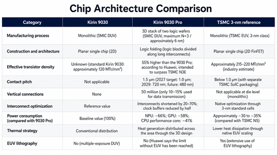
:quality(80)/p7i.vogel.de/wcms/4c/53/4c534208d09a9b1ce597938715e7fc19/0133288763v1.jpeg "Logic Folding: In its latest Kirin 9050 Pro, Huawei uses hybrid bonding to distribute the computing units across two silicon layers in order to increase the effective transistor density without resorting to finer manufacturing processes. (Image:Huawei)")
:quality(80)/p7i.vogel.de/wcms/56/d1/56d131e0b5bd05ef47411e92ad740cb4/0133351029v1.jpeg "Researchers at DTU have developed a nanolaser in a semiconductor membrane. The structure concentrates charge carriers and the light field into a small area (shaded in blue). If data is transmitted on microchips using light instead of electrical signals, transmission speeds can be increased and energy losses reduced. (Image:Yi Yu, DTU)")
:quality(80)/p7i.vogel.de/wcms/5e/55/5e55101ddc6338f755fcf3244db1367f/0133331863v1.jpeg "For data center projects, it is becoming increasingly important to also obtain the consent of the affected community. (Image:Dall-E / AI-generated)")
:quality(80)/p7i.vogel.de/wcms/8d/f9/8df95d3f58408673986b3d643e6b63ba/0133252773v1.jpeg "TXC targets high-speed optical links in AI data centers with 312.5 MHz oscillators, among other solutions. As data rates increase, requirements for jitter and frequency stability become more demanding as well. (Bild: TXC)")

:quality(80)/p7i.vogel.de/wcms/04/a5/04a55af7c725abd266c1afc3a4f494a8/0131668052v1.jpeg "TSMC CEO C.C. Wei sees a chip shortage on the global market for years to come, driven by the high demands of the ongoing AI boom. However, the company intends to keep prices stable despite fully utilized capacities. (Image:TMSC)")
Date: 08.12.2025
Naturally, we always handle your personal data responsibly. Any personal data we receive from you is processed in accordance with applicable data protection legislation. For detailed information please see our privacy policy.
Consent to the use of data for promotional purposes
I hereby consent to Vogel Communications Group GmbH & Co. KG, Max-Planck-Str. 7-9, 97082 Würzburg including any affiliated companies according to §§ 15 et seq. AktG (hereafter: Vogel Communications Group) using my e-mail address to send editorial newsletters. A list of all affiliated companies can be found here
Newsletter content may include all products and services of any companies mentioned above, including for example specialist journals and books, events and fairs as well as event-related products and services, print and digital media offers and services such as additional (editorial) newsletters, raffles, lead campaigns, market research both online and offline, specialist webportals and e-learning offers. In case my personal telephone number has also been collected, it may be used for offers of aforementioned products, for services of the companies mentioned above, and market research purposes.
Additionally, my consent also includes the processing of my email address and telephone number for data matching for marketing purposes with select advertising partners such as LinkedIn, Google, and Meta. For this, Vogel Communications Group may transmit said data in hashed form to the advertising partners who then use said data to determine whether I am also a member of the mentioned advertising partner portals. Vogel Communications Group uses this feature for the purposes of re-targeting (up-selling, cross-selling, and customer loyalty), generating so-called look-alike audiences for acquisition of new customers, and as basis for exclusion for on-going advertising campaigns. Further information can be found in section “data matching for marketing purposes”.
In case I access protected data on Internet portals of Vogel Communications Group including any affiliated companies according to §§ 15 et seq. AktG, I need to provide further data in order to register for the access to such content. In return for this free access to editorial content, my data may be used in accordance with this consent for the purposes stated here. This does not apply to data matching for marketing purposes.
Right of revocation
I understand that I can revoke my consent at will. My revocation does not change the lawfulness of data processing that was conducted based on my consent leading up to my revocation. One option to declare my revocation is to use the contact form found at https://contact.vogel.de. In case I no longer wish to receive certain newsletters, I have subscribed to, I can also click on the unsubscribe link included at the end of a newsletter. Further information regarding my right of revocation and the implementation of it as well as the consequences of my revocation can be found in the data protection declaration, section editorial newsletter.
:quality(80)/p7i.vogel.de/wcms/8e/44/8e44bf5fc8196c413fc1fd25814beab2/0131596875v1.jpeg "Huawei is exploring alternative ways to produce fast and advanced chips. (Image:Huawei)")
:quality(80)/p7i.vogel.de/wcms/e5/ec/e5ecd0db602320f5df17db00e3fc20a6/0131484998v1.jpeg "He Tingbo, President of Huawei's Semiconductor Business Unit, at the IEEE International Symposium on Circuits and Systems (ISCAS) 2026 in Shanghai. (Image:Huawei)")