Foundry BusinessRapidus Aims to Pressure TSMC with a 2nm Pricing Strategy
By
| Translated by AI
3 min Reading Time
Declaration of war in the foundry business: The Japanese contract manufacturer Rapidus aims to challenge industry leader TSMC in the 2nm foundry business through pricing. However, the roadmap to the targeted mass production in 2027 heavily depends on interested customers, yield proofs, and government funding.
With an ambitious pricing strategy, Rapidus, still a relatively young company as a contract manufacturer, aims to directly challenge the dominant competitor TSMC from Japan. However, apart from the technological race, the targeted goal heavily depends on customer demand and investments from the Japanese government.
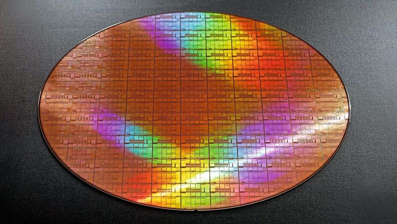
(Image: Rapidus)
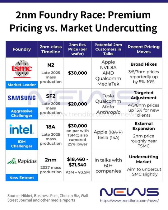
Rapidus positions itself in the race for leading logic processes with an aggressive pricing strategy. According to Nikkei, the Japanese foundry newcomer plans to offer its anticipated 2nm services at least at TSMC's price level or slightly below.
Rapidus cites a reference range of 3.0 to 3.5 million yen per wafer. This currently corresponds to approximately 18,500 to 21,500 USD, although exchange rates and customer-specific requirements may influence the final price.
This would position Rapidus significantly below the rumored prices of established providers. TSMC's 2nm process and Intel's 18A node are reported in industry reports to be around 30,000 USD per wafer, while Samsung's 2nm offering is estimated at approximately 20,000 USD.
Price Competition Meets Limited Capacities
The timing is strategically significant, as TSMC and Samsung are reportedly implementing price increases for several advanced nodes. At TSMC, increases of 5 to 10 percent are being reported for processes such as 3nm, 5nm, and 7nm, while Samsung is said to be raising new customer prices by around 15 percent for selected highly demanded nodes.
Rapidus is building its 2nm ambitions on the IIM-1 fab in Chitose, Hokkaido. The pilot line began operations in April 2025 after ASML delivered Japan's first mass-production-capable EUV system, the TWINSCAN NXE:3800E, at the end of 2024. The planned ramp-up is ambitious. Rapidus aims for mass production in the second half of fiscal year 2027 and plans to scale from around 6,000 wafer starts per month to approximately 25,000 wafer starts within the first year.
Technologically, the 2nm process is based on a gate-all-around nanosheet approach that emerged from cooperation with IBM. Rapidus engineers were trained for this at the Albany NanoTech Complex before the transfer to Chitose began.
Technology Alone Is Not Enough
As a differentiation feature, Rapidus points to a manufacturing concept with single-wafer front-end processing. Under the name Rapid and Unified Manufacturing Service, wafer data is to be fed into AI models to improve yield learning and throughput times. However, the crucial proof for industrial scaling is still missing. While Rapidus has reported a 2nm prototype with expected electrical properties, it has not yet published reliable yield data.
Financing remains another key issue. In February, Rapidus completed a funding round of 267.6 billion yen, with 100 billion yen coming from state funds and 167.6 billion yen from 32 private companies. Additionally, Japan has pledged extensive support for the coming years. The state's involvement makes Tokyo the largest single shareholder and grants the government special rights to influence key decisions such as technology partnerships or share transfers.
Planned timelines and pricing strategies for 2nm manufacturing processes from TSMC, Samsung Foundry, Intel Foundry, and Rapidus in comparison.
(Image: Trendforce)
According to CEO Atsuyoshi Koike, Rapidus is in talks with more than 60 companies, mostly from abroad. Preliminary price offers have reportedly been sent to around ten potential customers. Specific design partnerships exist with companies such as Tenstorrent and Esperanto Technologies, both focused on energy-efficient AI and RISC-V designs. However, binding high-volume orders that fully utilize the planned capacity would be crucial for the business model.
Japan's semiconductor strategy is thus running on two tracks. While TSMC's JASM plant in Kumamoto already serves mature nodes for automotive and industrial applications and prepares a second fab with more advanced nodes, Rapidus takes on the riskier part of the national return to the leading edge.
Long-term, Rapidus is aiming for 1.4nm by 2029, operational profitability by fiscal year 2030, and an IPO in fiscal year 2031. Whether this roadmap is feasible depends mainly on three points: a named volume customer, reliable yield progress at 2nm, and proof that the fab in Chitose reaches the planned capacity ramp.
Date: 08.12.2025
Naturally, we always handle your personal data responsibly. Any personal data we receive from you is processed in accordance with applicable data protection legislation. For detailed information please see our privacy policy.
Consent to the use of data for promotional purposes
I hereby consent to Vogel Communications Group GmbH & Co. KG, Max-Planck-Str. 7-9, 97082 Würzburg including any affiliated companies according to §§ 15 et seq. AktG (hereafter: Vogel Communications Group) using my e-mail address to send editorial newsletters. A list of all affiliated companies can be found here
Newsletter content may include all products and services of any companies mentioned above, including for example specialist journals and books, events and fairs as well as event-related products and services, print and digital media offers and services such as additional (editorial) newsletters, raffles, lead campaigns, market research both online and offline, specialist webportals and e-learning offers. In case my personal telephone number has also been collected, it may be used for offers of aforementioned products, for services of the companies mentioned above, and market research purposes.
Additionally, my consent also includes the processing of my email address and telephone number for data matching for marketing purposes with select advertising partners such as LinkedIn, Google, and Meta. For this, Vogel Communications Group may transmit said data in hashed form to the advertising partners who then use said data to determine whether I am also a member of the mentioned advertising partner portals. Vogel Communications Group uses this feature for the purposes of re-targeting (up-selling, cross-selling, and customer loyalty), generating so-called look-alike audiences for acquisition of new customers, and as basis for exclusion for on-going advertising campaigns. Further information can be found in section “data matching for marketing purposes”.
In case I access protected data on Internet portals of Vogel Communications Group including any affiliated companies according to §§ 15 et seq. AktG, I need to provide further data in order to register for the access to such content. In return for this free access to editorial content, my data may be used in accordance with this consent for the purposes stated here. This does not apply to data matching for marketing purposes.
Right of revocation
I understand that I can revoke my consent at will. My revocation does not change the lawfulness of data processing that was conducted based on my consent leading up to my revocation. One option to declare my revocation is to use the contact form found at https://contact.vogel.de. In case I no longer wish to receive certain newsletters, I have subscribed to, I can also click on the unsubscribe link included at the end of a newsletter. Further information regarding my right of revocation and the implementation of it as well as the consequences of my revocation can be found in the data protection declaration, section editorial newsletter.



:quality(80)/p7i.vogel.de/wcms/5f/96/5f9606264f35f5979529286a887bbccf/0133859498v1.jpeg "Trumpf Expands Its Portfolio for 2D Laser Cutting (Image:TRUMPF GMBH + CO. KG)")
:quality(80)/p7i.vogel.de/wcms/ed/78/ed786ed6b280ff6c692908f01f715e3d/0113143253v1.jpeg "In our China Market Insider, we regularly provide you with relevant information straight from China. (Image:© Eisenhans - stock.adobe.com)")
:quality(80)/p7i.vogel.de/wcms/68/a5/68a5ce0896756c1dcf48dbeceefafbd3/0132300990v1.jpeg "Christoph Geigges is President and CEO of Walter AG. Headquartered in Tübingen (Germany), the company is one of the world’s leading suppliers of precision tools for metalworking. Under Geigges’ leadership, this long-established company is increasingly transforming itself from a tool manufacturer into an engineering partner that supports the entire manufacturing process. (Image: Walter AG)")
:quality(80)/p7i.vogel.de/wcms/3e/7c/3e7c26f44c68545fc7318597b6b65903/0133649650v1.jpeg "The flexible Heller circular storage system can store and process pallets measuring both 630 millimeters by 630 millimeters and 800 millimeters by 800 millimeters—even in mixed-mode operation. This makes the entire production line particularly flexible. (Image:Brighter)")
:quality(80)/p7i.vogel.de/wcms/87/88/8788e0b7fd98cca21a9c370ed0f0aa18/0133859688v1.jpeg "The software newly developed at Fraunhofer IWU helps employees reliably
identify parts that do not meet quality requirements. (Image:Fraunhofer IWU)")
:quality(80)/p7i.vogel.de/wcms/4b/7c/4b7c11f510878f154012d04c18a7c3cc/0133798118v1.jpeg "RobCo Becomes a Unicorn: The Munich-based robotics company has reached a valuation of more than one billion U.S. dollars and is driving the next generation of autonomous industrial robotics with Alfie. (Image:RobCo)")
:quality(80)/p7i.vogel.de/wcms/c8/a9/c8a96d5841d508c9e9c609c64168cbaa/0133758997v1.jpeg "Hospital Robotics: Neura Robotics' autonomous healthcare platform is designed to independently transport empty hospital beds between wards and floors. (Image:Neura Robotics)")
:quality(80)/p7i.vogel.de/wcms/88/dc/88dc38a1a0b5e016192ab83b0850fbd0/0133514708v1.jpeg "Scalable data sovereignty is the foundation for the transition from computationally intensive AI processing and growing data streams to sustainable, energy-efficient storage systems. (Image:Gemini / AI-generated)")
:quality(80)/p7i.vogel.de/wcms/a7/8a/a78a582a42a96aaaff38bd6b8f97a015/vishal-lal-mit-kernuhrv1.jpeg "It's ticking: Researchers have stabilized the first atomic clock. (Source: PTB)")
:quality(80)/p7i.vogel.de/wcms/36/f9/36f96a206fc408c9a632ce849de1f7fa/newsimage428299v1.jpeg "Polystyrene is used in protective packaging for televisions and electronic devices, in decorative moldings and baseboards for interior home construction, and even in Petri dishes. (Source: Hereon/Marcel Schwickerath)")
:quality(80)/p7i.vogel.de/wcms/90/30/90300137452b00d22f95113eff065ac3/fliehkraftkupplungen-und-bremsen-montage-centrifugal-clutches-and-brakes-assembly-1v1.jpeg "Installation: Centrifugal clutches should always be precisely matched to the machine. (Source: Amsbeck Machine Technology)")
:quality(80)/p7i.vogel.de/wcms/93/84/9384230e840a99a2015fdd3e0af11e2b/newsimage428236v1.jpeg "The crutch replicates the natural, biomechanical movement pattern of the human body. (Source: Leon Kast)")
:quality(80)/p7i.vogel.de/wcms/50/23/5023ffaefac8f9a47286b368143b88eb/0133801078v1.jpeg "Life isn't exactly a walk in the park for Porsche right now. And now Porsche management is saying that next year will be even worse. Read here to find out why that's supposed to be the case... (Image: Porsche)")
:quality(80)/p7i.vogel.de/wcms/2f/ab/2fabf62cdd2f57cb279e00931c91c869/0133794991v1.jpeg "The Atto 2 SUV is one of BYD's most popular plug-in hybrids. (Image:BYD)")
:quality(80)/p7i.vogel.de/wcms/e9/6e/e96e34d467ca1017f2a689275ae07302/0133815122v1.jpeg "Porsche CEO Leiters has shared new information about the company's model plans. (Image:Porsche)")
:quality(80)/p7i.vogel.de/wcms/0a/50/0a50938be0b598b36efc4e5457ed56dd/forvia-siege-zen-massage-16-9-06v1.jpeg "Seat with massage function by Forvia. (Source: Forvia)")
:quality(80)/p7i.vogel.de/wcms/4d/eb/4debf44ac7c0349544c70033bb9a182c/0133750488v1.jpeg "AI-enabled hardware: is a prerequisite for successful AI projects. (Image:Tung Lam)")
:quality(80)/p7i.vogel.de/wcms/36/f0/36f0472d20227013871aa790f4d48ac6/0133726018v1.jpeg "Ion beams can ablate, coat, or smooth surfaces down to the atomic level. Such processes are used, among other things, in optical chips, precision optics, and superconducting materials. (Image:AI-generated)")
:quality(80)/p7i.vogel.de/wcms/1f/47/1f47da6ee12c38a745eb478a04157a65/0133726100v1.jpeg "The schematic diagram shows the structure of a 3D NAND memory device with memory cells stacked on top of one another and vertical connections for high storage density. (Image:Dall-E / AI-generated)")
:quality(80)/p7i.vogel.de/wcms/b6/06/b6060e0b986e103e442b3971b6c0724c/0133731535v1.jpeg "Rendering of the planned Terafab facility in Texas (presumably generated using AI). Elon Musk does not seem to be making progress with his plans to operate his own semiconductor manufacturing facility. The SpaceX CEO has confirmed that he is currently in talks with TSMC regarding a stake in the Terafab project. (Image:SpaceX)")
:quality(80)/p7i.vogel.de/wcms/19/d2/19d29497395712a79307f99445b41e48/0131825683v1.jpeg "Figure 1: (A) X-Cut HAADF scanning electron microscopy image of a WS2 device with a CPP of 50 nm, a contact length of 19 nm, and a width of 256 nm after etching the gate interconnect. (B) The corresponding energy-dispersive X-ray spectroscopy (EDS) analysis (Image:Imec)")
:quality(80)/p7i.vogel.de/wcms/5b/38/5b385ec75bff6e84b70a02c0c939dd2b/0129331527v1.jpeg "The TSMC site of Japan Advanced Semiconductor Manufacturing in Kumamoto, Japan. While the second fab currently under construction was initially only intended for the production of semiconductors using the N6 process, the contract manufacturer is currently negotiating with the Japanese government to possibly upgrade the site to N3 after all. (Image:JASM)")
:quality(80)/p7i.vogel.de/wcms/b4/a8/b4a82a0f554fd526f6deff1561aa5847/0128153246v1.jpeg "Samsung began chip production in summer 2022 using 3-nm process technology with GAA architecture. (Image:Samsung)")