Gallium Oxide Power SemiconductorVertical Gallium Oxide MOSFET Reaches 1.2 Amperes
From
Dipl.-Ing. (FH) Michael Richter
| Translated by AI
4 min Reading Time
A normally-off gallium oxide MOSFET combines a 1.2 A on-state current with more than 900 V breakdown voltage. New cell structures and an implantation process are intended to enable the development of more powerful devices.
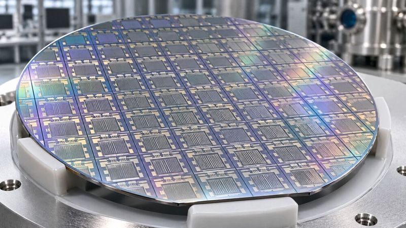
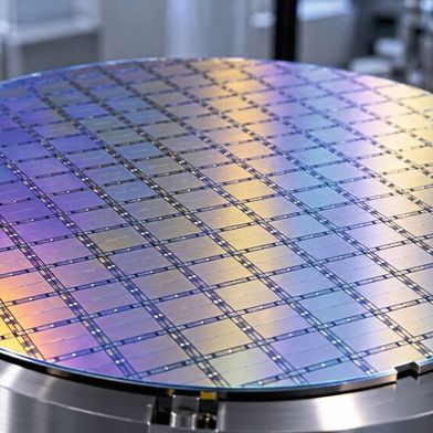
Structured semiconductor wafer as a symbol of the development of new power switches. Vertical gallium oxide MOSFETs are intended to combine high blocking voltages with increasing current-carrying capacity. (Stock image)
(Image: Dall-E / AI-generated)
A vertical gallium oxide MOSFET from Shanghai has achieved an on-state current of 1.2 A and a breakdown voltage of more than 900 V, according to its development team. This is reported by the Chinese newspaper Science and Technology Daily, citing Shanghai Jiachi Power Technology. The company has completed an initial round of fabrication and characterization. Based on its own analysis of published results, it claims the world’s first vertical gallium oxide MOSFET with an on-state current above 1 A. [1]
Why Vertical Construction is Relevant
In vertical power transistors, the current flows through the depth of the semiconductor. In the off state, a drift region takes on a substantial part of the voltage blocking. This arrangement fundamentally offers good conditions for combining high blocking voltages with current-carrying capability that can be scaled via the chip area. Vertical gallium oxide MOSFETs are not a new concept: as early as 2018, the Japanese research institute NICT and the Tokyo University of Agriculture and Technology reported on a transistor manufactured using ion implantation. The newly asserted claim to primacy therefore relates to surpassing the ampere threshold. [2]
Gallium oxide is of interest for power electronics because of its wide bandgap and high theoretical breakdown field strength. At the same blocking voltage, the material fundamentally offers the possibility of reducing the resistance of the drift region. Whether this results in a more efficient device, however, also depends on the channel, contacts, switching behavior, and heat dissipation. A material advantage is therefore not yet proof of lower losses in a real converter. [3]
Self-Locking Through an Adapted Structure and Manufacturing
Jiachi specifies a threshold voltage of 3.9 V. The transistor therefore operates in enhancement mode and is normally off at a gate-source voltage of 0 V. As the technical basis, the development team describes new MOSFET cell and edge termination structures as well as a self-aligned ion implantation process for channel formation. These are intended to make the geometry, the doping profile, and the electric field distribution more precisely controllable. [1]
The report puts the progress into context with the difficult p-type doping of gallium oxide. However, this does not allow the conclusion that a technically usable p-type conduction in gallium oxide has now been demonstrated. Which dopants and channel mechanisms the new transistor uses remains unclear. Normally-off operation alone does not prove successful p-type doping: research also investigates structures that bypass this requirement through their geometry. [3]
What the Electrical Characteristic Values Indicate
The company specifies the specific on-state resistance as 33 mΩ·cm². This area-related characteristic value must be distinguished from the absolute on-state resistance in ohms. Without the corresponding reference area, no component resistance can be derived from it, and therefore no concrete conduction loss power can be calculated.
The demonstrator was designed for a voltage class of 750 V. In addition to the measured breakdown voltage above 900 V, a leakage current of less than 3 µA is stated. [1] However, the breakdown voltage is not an approval for continuous operation at this value. The leakage current can only be reliably compared with other technologies once the test voltage, temperature, and component area are known.
Essential boundary conditions for the inrush current are also missing, including gate voltage, temperature, and the distinction between pulsed and continuous operation. The 1.2 A therefore initially represents a reported measured value, not a fully specified continuous current capability. For an assessment in switching operation, additional information would be required as well, such as switching energies, capacitances, and the stability of the threshold voltage.
Heat Dissipation Determines the Practical Usefulness
A key challenge remains the low, direction-dependent thermal conductivity of β-gallium oxide. Waste heat must be dissipated in such a way that local overheating does not limit current carrying capability and reliability. Scientific studies on vertical gallium oxide structures therefore show how strongly thermal performance depends on the device geometry and the proximity of cooling to the heat source. [3]
Date: 08.12.2025
Naturally, we always handle your personal data responsibly. Any personal data we receive from you is processed in accordance with applicable data protection legislation. For detailed information please see our privacy policy.
Consent to the use of data for promotional purposes
I hereby consent to Vogel Communications Group GmbH & Co. KG, Max-Planck-Str. 7-9, 97082 Würzburg including any affiliated companies according to §§ 15 et seq. AktG (hereafter: Vogel Communications Group) using my e-mail address to send editorial newsletters. A list of all affiliated companies can be found here
Newsletter content may include all products and services of any companies mentioned above, including for example specialist journals and books, events and fairs as well as event-related products and services, print and digital media offers and services such as additional (editorial) newsletters, raffles, lead campaigns, market research both online and offline, specialist webportals and e-learning offers. In case my personal telephone number has also been collected, it may be used for offers of aforementioned products, for services of the companies mentioned above, and market research purposes.
Additionally, my consent also includes the processing of my email address and telephone number for data matching for marketing purposes with select advertising partners such as LinkedIn, Google, and Meta. For this, Vogel Communications Group may transmit said data in hashed form to the advertising partners who then use said data to determine whether I am also a member of the mentioned advertising partner portals. Vogel Communications Group uses this feature for the purposes of re-targeting (up-selling, cross-selling, and customer loyalty), generating so-called look-alike audiences for acquisition of new customers, and as basis for exclusion for on-going advertising campaigns. Further information can be found in section “data matching for marketing purposes”.
In case I access protected data on Internet portals of Vogel Communications Group including any affiliated companies according to §§ 15 et seq. AktG, I need to provide further data in order to register for the access to such content. In return for this free access to editorial content, my data may be used in accordance with this consent for the purposes stated here. This does not apply to data matching for marketing purposes.
Right of revocation
I understand that I can revoke my consent at will. My revocation does not change the lawfulness of data processing that was conducted based on my consent leading up to my revocation. One option to declare my revocation is to use the contact form found at https://contact.vogel.de. In case I no longer wish to receive certain newsletters, I have subscribed to, I can also click on the unsubscribe link included at the end of a newsletter. Further information regarding my right of revocation and the implementation of it as well as the consequences of my revocation can be found in the data protection declaration, section editorial newsletter.
The reported transistor is therefore a development step toward more robust vertical gallium oxide switches. Superiority over commercial SiC MOSFETs has not yet been demonstrated with the published information. What is missing above all are comparable operating conditions as well as data on dynamic losses and reliability. The decisive factor will be whether the achieved electrical characteristics can also be confirmed at higher temperature, under repeated switching, and in reproducible manufacturing. (mr)
[1] Science and Technology Daily, Wang Chun, 29. September 2026: https://www.stdaily.com/web/gdxw/2026-09/29/content_590062.html
[2] NICT / Tokyo University of Agriculture and Technology, 12. Dezember 2018: Vertical Ga₂O₃ Transistor through Ion Implantation Doping. https://www.nict.go.jp/en/press/2018/12/12-1.html
[3] „Thermal management strategies for gallium oxide vertical trench-fin MOSFETs“, Journal of Applied Physics 129, 085301 (2021), https://pubs.aip.org/aip/jap/article/129/8/085301/565815/Thermal-management-strategies-for-gallium-oxide