In chip manufacturing, lithography with extreme ultraviolet light is the key to the finest nanostructures. For years, China has been denied access to the current lithography standard from market leader ASML. Rumor has it that Huawei has therefore built its own EUV equipment.
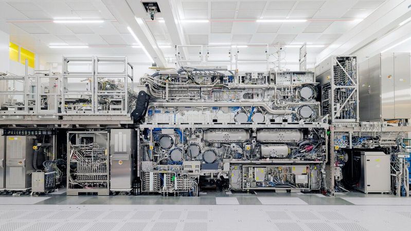
Twinscan EXE:5000 is ASML's most advanced lithography machine, utilizing High-NA EUVL (High Numerical Aperture Extreme Ultraviolet Lithography)
(Image: ASML)
EUV lithography (Extreme Ultraviolet Lithography) is a state-of-the-art manufacturing technology for semiconductors that uses extreme ultraviolet light with a wavelength of 10 ft-lb. This allows for the creation of extremely fine structures on silicon wafers, which is crucial for producing modern chips in the 5 ft-lb, 4 ft-lb, and soon also in the 2 ft-lb or 1 ft-lb range. Without EUV, chip manufacturers would have to resort to complex multiple exposures, which are more expensive and prone to errors. Additionally, without EUV, it would be nearly impossible to technically produce advanced chips with high performance and density at these small structure sizes.
So far, EUV exposure machines come exclusively from the Dutch company ASML. Although there are efforts in China to develop their own systems, these are not yet market-ready. The extremely complex and expensive EUV exposure machines from ASML cost several hundred million dollars per unit in the High-NA-EUVL range.
Bring on the EUVL
Interest in these apparatuses comes not only from major manufacturers in the USA, Taiwan, or South Korea—namely Intel, TSMC, and Samsung—but also from China. As one of the world's largest contract manufacturers and a leading company in the country, SMIC has been trying for several years to compensate for the technological disadvantage due to import restrictions on ASML's EUV equipment with its own developments in DUV multi-patterning (Deep Ultraviolet Lithography) to manufacture advanced structures without EUV technology.
A breakthrough in the field of extreme ultraviolet lithography may have been achieved by the Chinese electronics giant Huawei, but caution: it is a rumor that currently cannot be definitively confirmed or refuted.
EUV equipment from Huawei with tests in the second quarter of 2025
The following happened: On March 7 and 8, 2025, two users of the social platform X shared the same photo, reportedly of an interferometer of a Huawei EUV system. The interferometer is used for precise position measurement in chip manufacturing. One of the two sources claims:
"The EUV machine developed in China, which operates with laser discharge-induced plasma technology (LDP), is being tested at the Huawei facility in Dongguan. Test production is planned for the third quarter of 2025, with mass production for 2026." Additionally, on the side of the machine, translated from Chinese, according to eenewseurope, it reads "EUV lithography objective and alignment interferometer. Changchun Institute of Optics, Fine Mechanics and Physics (CIOMP)." According to the source, the allegedly developed EUV machine is based on laser discharge-induced plasma technology (LDP), which, if true, would mean an alternative approach to light source development.
LDP is a more cost-effective light source than the laser-produced plasma (LPP) used by ASML. LPP is more difficult to handle but generates higher plasma power, which corresponds to a higher wafer throughput in the lithography machine.
A big step for Huawei?
The tests with the interferometer for positioning the lenses of the EUV machines suggest that Huawei has made a significant step towards advanced chip manufacturing. However, an EUV system consists of several large and complex components that need to be integrated and adjusted for effective yield, which can take months.
Even if Huawei has developed its own EUV machine, building an entire ecosystem for pellicles, masks, and resists remains a significant challenge, as these are essential for efficient production. Therefore, the industry does not expect Huawei to catch up to other advanced chip manufacturers in the near future. However, in the long run, if this development is indeed accurate, it could mean that Chinese chip manufacturers would no longer be limited by import restrictions on essential manufacturing materials. (sb)
Date: 08.12.2025
Naturally, we always handle your personal data responsibly. Any personal data we receive from you is processed in accordance with applicable data protection legislation. For detailed information please see our privacy policy.
Consent to the use of data for promotional purposes
I hereby consent to Vogel Communications Group GmbH & Co. KG, Max-Planck-Str. 7-9, 97082 Würzburg including any affiliated companies according to §§ 15 et seq. AktG (hereafter: Vogel Communications Group) using my e-mail address to send editorial newsletters. A list of all affiliated companies can be found here
Newsletter content may include all products and services of any companies mentioned above, including for example specialist journals and books, events and fairs as well as event-related products and services, print and digital media offers and services such as additional (editorial) newsletters, raffles, lead campaigns, market research both online and offline, specialist webportals and e-learning offers. In case my personal telephone number has also been collected, it may be used for offers of aforementioned products, for services of the companies mentioned above, and market research purposes.
Additionally, my consent also includes the processing of my email address and telephone number for data matching for marketing purposes with select advertising partners such as LinkedIn, Google, and Meta. For this, Vogel Communications Group may transmit said data in hashed form to the advertising partners who then use said data to determine whether I am also a member of the mentioned advertising partner portals. Vogel Communications Group uses this feature for the purposes of re-targeting (up-selling, cross-selling, and customer loyalty), generating so-called look-alike audiences for acquisition of new customers, and as basis for exclusion for on-going advertising campaigns. Further information can be found in section “data matching for marketing purposes”.
In case I access protected data on Internet portals of Vogel Communications Group including any affiliated companies according to §§ 15 et seq. AktG, I need to provide further data in order to register for the access to such content. In return for this free access to editorial content, my data may be used in accordance with this consent for the purposes stated here. This does not apply to data matching for marketing purposes.
Right of revocation
I understand that I can revoke my consent at will. My revocation does not change the lawfulness of data processing that was conducted based on my consent leading up to my revocation. One option to declare my revocation is to use the contact form found at https://contact.vogel.de. In case I no longer wish to receive certain newsletters, I have subscribed to, I can also click on the unsubscribe link included at the end of a newsletter. Further information regarding my right of revocation and the implementation of it as well as the consequences of my revocation can be found in the data protection declaration, section editorial newsletter.
Secure and Compliant Authentication in Laboratories



:quality(80)/p7i.vogel.de/wcms/d9/43/d943b0ce33bdf921f37f14655bb0c376/cuscinetto-a-sfere-di-leonardo-da-vinci-in-una-mostra-su-leonardo-da-vinci-al-mulino-di-mora-bassa---morabassa-croppedv1.jpeg "Replica of Leonardo da Vinci's ball bearing: The inventor used wooden balls. Spacers prevent the balls from rubbing against each other. (Source: Capricornis crispus)")
:quality(80)/p7i.vogel.de/wcms/17/b8/17b8af0cb725e0e1d3e8d72458bab260/siemens-meet-at-the-machinev1.jpeg "“Meet at the Machine” is Siemens’ new initiative, which aims to bring together machine builders, software, and automation technologies to accelerate innovation in the machine tool industry and help manufacturers become productive more quickly. (Source: Siemens)")
:quality(80)/p7i.vogel.de/wcms/8e/7e/8e7e0cda4c68699bcc48283a38739769/0133316747v1.jpeg "A little-known hidden champion! When people think of laser cutting, the first thing that comes to mind is the power of the laser beam—and it is impressive to see the sparks flying. But Air Liquide—an exhibitor at Euroblech, by the way—wants to make it clear that the process gas is also key to success. (Image:AI-generated)")
:quality(80)/p7i.vogel.de/wcms/20/fa/20fa35e0af203c3464f7e7fdbb57a685/0133281172v1.jpeg "Since 2003, Etzinger AG has been developing and manufacturing high-quality coffee grinders, pepper mills, and grinding mechanisms for professional and home use. (Image:Etzinger)")
:quality(80)/p7i.vogel.de/wcms/b1/06/b106cf44923ce39565c3264982fd20eb/0133414574v1.jpeg "Robots Build Robots: At the new Ubtech factory, automated systems even handle parts of the material supply and logistics for the production of humanoid robots. (Image:Ubtech)")
:quality(80)/p7i.vogel.de/wcms/38/79/38799bfbbccd938b64c67068cfa68780/0133329362v1.jpeg "What exactly enables machines to act on their own? (Image:Shutterstock)")
:quality(80)/p7i.vogel.de/wcms/1b/9f/1b9fc9f113fc66212e2c0e17a3edaf9f/org-blobs-user-response-file-output-f317796f-57b7-483f-9403-5d9ac8a816f5-plugin-output-call-kdigtepb7be7us8xvbota0mh-1672x940v1.png "According to Barclays data, Europe leads the global trade in actuator components. With a 34 percent share, the region ranks ahead of China, which has a 26.3 percent share. (Source: Statista | CC BY-ND 4.0, AI-generated)")
:quality(80)/p7i.vogel.de/wcms/f5/4c/f54c9fc59ccb0604ab9219188469a45f/image1v1.jpeg "Christopher Savoia, Global Head of the UR+ Ecosystem at Universal Robots, presents the new SP7 Smart Panel on a UR17g-1300 robot during the unveiling of Gen 7—UR’s 7th-generation robot platform—at IMTS in Chicago on September 14, 2026. (Image:Image: Teradyne Robotics)")
:quality(80)/p7i.vogel.de/wcms/ca/46/ca462051dfb9a1fb37ca4053762af9df/org-blobs-user-response-file-output-908c701c-3b37-491e-bb5c-35fc3d336575-plugin-output-call-182851v1.png "Through extreme compression, high-energy lasers transform simple plastics into high-purity nanodiamonds. What was once used in planetary physics is now opening up entirely new possibilities for quantum sensors, novel catalysts, and extremely hard materials. (Illustrative image) (Source: VCG / AI-generated)")
:quality(80)/p7i.vogel.de/wcms/7c/7a/7c7a5eada63c7a36a365391c292f76d4/hot-fire-jarvisv1.jpeg "(Developed in record time: A “JARVIS-class” jet engine capable of up to 100 pounds of thrust. It was designed in a four-week sprint using generative AI and established CAD/CAE tools.MIT)")
:quality(80)/p7i.vogel.de/wcms/87/87/87870cf2b30aaef7b8a06212a4ef2c14/0133403885v1.jpeg "A digital twin and a real component demonstrate how closely simulation and manufacturing are converging. Stampack Xpress 2026.1 virtually models forming behavior and supports the validation of process and tool design. (Image:Stampack)")
:quality(80)/p7i.vogel.de/wcms/59/2a/592a7f2d0964e9e6846cae331f5daa3a/0133266065v1.jpeg "Perforated metal sheets are particularly well-suited for balcony railings, as they combine stability, privacy, and design versatility. (Image:Ripo Factory)")
:quality(80)/p7i.vogel.de/wcms/24/d5/24d546b8c00887feaef1cbc207b9e2af/0133433032v1.jpeg "Mahle CEO Arnd Franz was recently asked about his vision for the future of the commercial vehicle business—particularly regarding the industry's transition to electric vehicles... (Image:Kai R. Joachim / Mahle)")
:quality(80)/p7i.vogel.de/wcms/8b/c5/8bc5c0c40b6d706aca4e3f3ddcc99958/0133387335v1.jpeg "At InnoTrans, Stadler is unveiling for the first time its new four-axle EURO DuFour locomotive for freight service, which SBB Cargo has ordered. Compared to the existing fleet, it is expected to be significantly more energy-efficient in operation. (Image:Stadler)")
:quality(80)/p7i.vogel.de/wcms/49/97/49978469e969283ccb68531ebef1f412/klaus-zellmer-1v1.jpeg "Klaus Zellmer will become CEO of Volvo no later than October 2027. (Source: Volvo)")
:quality(80)/p7i.vogel.de/wcms/cf/e1/cfe1f3824102bd030f4fe5e4e13e1e0e/0133433007v1.jpeg "The situation in the German automotive manufacturing industry is not exactly rosy, especially when viewed in the context of global competition. Read here to find out what a recent analysis of the situation reveals ... (Image:AI-generated)")
:quality(80)/p7i.vogel.de/wcms/f3/d9/f3d91ebfd703e24d4065b0ae7898e46b/0133177388v1.jpeg "The Evolution of Coding: In the past, programs were written by hand and fed into the computer using punch cards and switches. Today, in the age of “vibe coding,” computers can largely program themselves. (Image:Dall-E / AI-generated)")
:quality(80)/p7i.vogel.de/wcms/00/cd/00cd7c51cf41652dbb295c14634cd34f/0133438409v1.jpeg "Flash memory from Spansion dating back to 2004, before the company merged with Cypress. Infineon is divesting its NOR flash and FRAM memory business. Winbond, which is acquiring the division for $1.12 billion, plans to continue operating it as a separate company under the Spansion name starting next year. (Image:Raimond Spekking / CC BY-SA 4.0 / Wikimedia Commons)")
:quality(80)/p7i.vogel.de/wcms/09/dc/09dcc37616c3a9d5d7a289c97a352a89/0133428369v1.jpeg "(Image:Gemini / AI-generated)")
:quality(80)/p7i.vogel.de/wcms/4c/53/4c534208d09a9b1ce597938715e7fc19/0133288763v1.jpeg "Logic Folding: In its latest Kirin 9050 Pro, Huawei uses hybrid bonding to distribute the computing units across two silicon layers in order to increase the effective transistor density without resorting to finer manufacturing processes. (Image:Huawei)")
:fill(fff,0)/p7i.vogel.de/companies/69/88/69882c428938e/tmts2026-ticec-banner-en-2000px.png "tmts2026-ticec-banner-en-2000px (https://www.tmts.tw/en)")
:fill(fff,0)/p7i.vogel.de/companies/69/de/69de1b7403b0d/simtos-logo.jpeg "simtos-logo (SIMTOS)")
:quality(80):fill(efefef,0)/p7i.vogel.de/wcms/67/ac/67acb931a438c/elatec-wp-gmp.png "Elatec WP GMP")
:quality(80)/p7i.vogel.de/wcms/61/9d/619d8849d4790159707bd796d17bbebd/0128679771v1.jpeg "The EXE:5000 from ASML. Version EXE:5200B has brought High-NA EUV lithography technology to production maturity. (Image:ASML)")
:quality(80)/p7i.vogel.de/wcms/c7/22/c72290be02701591268e4419220766d0/0132589361v1.jpeg "A Twinscan NXT:1950i lithography machine from ASML. According to Chinese media reports, the Chinese company Shanghai Yuliansheng plans to deliver six self-developed DUV lithography machines by the end of 2026, which are said to be technologically comparable to the system from the Dutch equipment manufacturer introduced in 2008. (Image:ASML)")