With structure sizes of 2 nm (0.08 µin) and below, traditional transistor scaling is increasingly reaching physical and economic limits. The next wave of innovation is therefore no longer driven solely by smaller transistors but by their intelligent integration. Advanced packaging is evolving from a downstream manufacturing step to a key technology for AI processors, chiplet architectures, and high-performance systems.
After Moore's Law: Packaging is becoming the most important driver for semiconductor technology.
For decades, Moore's Law was considered the benchmark for the semiconductor industry. The continuous increase in transistor density enabled higher computing performance while simultaneously reducing costs. However, with structure sizes of 2 nm and below, this progress is increasingly reaching physical and economic limits. Manufacturing processes are becoming more complex, while investments in new technologies are rising disproportionately.
This is also changing the way future performance improvements are achieved. Instead of solely accommodating more transistors on the same chip area, the focus is shifting to integrating multiple specialized semiconductors into a single package. Modern packaging technologies thus open up an additional dimension of scaling: system performance is no longer determined solely by transistor density but by the intelligent integration of different functions.
AI Makes Advanced Packaging a Key Technology
AI applications, in particular, are driving this change. Training large language models and other AI applications requires increasingly higher computing power, greater memory bandwidth, and maximum energy efficiency. Processors and high-performance memory must work much more closely together than before.
Advanced packaging provides the technological foundation for this. Interposers and through-silicon vias (TSV) significantly shorten the electrical signal paths between processors and memory modules. This reduces latency, parasitic effects, and energy losses, while simultaneously increasing the available bandwidth. As a result, performance improvements are increasingly achieved at the system level rather than solely through faster individual chips.
From Monolithic Chip to Chiplet System
At the same time, the architectural concepts of modern semiconductors are evolving. In 3D stacking, multiple dies are stacked vertically to achieve maximum integration densities. In contrast, package-level scaling follows a modular approach: several specialized chiplets are combined within a single package to form a powerful overall system. Both concepts enable higher computational density, more memory bandwidth, and improved energy efficiency.
The importance of these technologies is now also reflected in global investments. Singapore is expanding its research infrastructure for advanced packaging, Malaysia is increasing its manufacturing capacities, Japan is investing in next-generation packaging technologies, and India is emerging as a new production hub. At the same time, advanced packaging is becoming a central focus in the long-term strategies of foundries, memory manufacturers, and OSAT companies (Outsourced Semiconductor Assembly and Test).
Precision Manufacturing in the Micrometer Range
However, with three-dimensional integration, manufacturing requirements also increase. During die-to-wafer bonding, small voids form between the individual dies that need to be compensated. The mismatch causes mechanical stresses, which increase the risk of crack formation as the stack height grows. This must be addressed during manufacturing through additional measures to reduce residual stresses.
Wafer-to-wafer bonding largely avoids this issue but requires nearly perfect planarization of both wafers. Even slight distortions can affect the bonding process. Methods for stress and distortion compensation ensure that the necessary planarization is maintained during manufacturing.
At a glance
Advanced packaging is evolving from a traditional manufacturing step to the central interface of modern semiconductor systems. Drivers include AI applications, chiplet architectures, and increasing demands for memory bandwidth and energy efficiency. Techniques such as TSV, fine-pitch interconnects, and hybrid bonding enable significantly higher integration density. At the same time, they are transforming development processes and supply chains across the entire semiconductor industry.
At the same time, the demand for productivity and process stability is growing. Manufacturing operates in the micrometer range while still needing to achieve high throughput rates. Modern production equipment, therefore, continuously monitors critical process parameters using integrated sensors and inline metrology. Real-time analysis detects process deviations early, which plays a crucial role in minimizing yield losses.
Date: 08.12.2025
Naturally, we always handle your personal data responsibly. Any personal data we receive from you is processed in accordance with applicable data protection legislation. For detailed information please see our privacy policy.
Consent to the use of data for promotional purposes
I hereby consent to Vogel Communications Group GmbH & Co. KG, Max-Planck-Str. 7-9, 97082 Würzburg including any affiliated companies according to §§ 15 et seq. AktG (hereafter: Vogel Communications Group) using my e-mail address to send editorial newsletters. A list of all affiliated companies can be found here
Newsletter content may include all products and services of any companies mentioned above, including for example specialist journals and books, events and fairs as well as event-related products and services, print and digital media offers and services such as additional (editorial) newsletters, raffles, lead campaigns, market research both online and offline, specialist webportals and e-learning offers. In case my personal telephone number has also been collected, it may be used for offers of aforementioned products, for services of the companies mentioned above, and market research purposes.
Additionally, my consent also includes the processing of my email address and telephone number for data matching for marketing purposes with select advertising partners such as LinkedIn, Google, and Meta. For this, Vogel Communications Group may transmit said data in hashed form to the advertising partners who then use said data to determine whether I am also a member of the mentioned advertising partner portals. Vogel Communications Group uses this feature for the purposes of re-targeting (up-selling, cross-selling, and customer loyalty), generating so-called look-alike audiences for acquisition of new customers, and as basis for exclusion for on-going advertising campaigns. Further information can be found in section “data matching for marketing purposes”.
In case I access protected data on Internet portals of Vogel Communications Group including any affiliated companies according to §§ 15 et seq. AktG, I need to provide further data in order to register for the access to such content. In return for this free access to editorial content, my data may be used in accordance with this consent for the purposes stated here. This does not apply to data matching for marketing purposes.
Right of revocation
I understand that I can revoke my consent at will. My revocation does not change the lawfulness of data processing that was conducted based on my consent leading up to my revocation. One option to declare my revocation is to use the contact form found at https://contact.vogel.de. In case I no longer wish to receive certain newsletters, I have subscribed to, I can also click on the unsubscribe link included at the end of a newsletter. Further information regarding my right of revocation and the implementation of it as well as the consequences of my revocation can be found in the data protection declaration, section editorial newsletter.
Hybrid Bonding Opens Up New Integration Densities
With increasing integration density, thermal management and reliability come even more into focus. High-performance memory like High-Bandwidth Memory (HBM) already consists of stacks with up to 16 dies. Future generations will further increase this number, thereby intensifying the demands on heat dissipation and mechanical stability.
In heterogeneous architectures, processors, memory, photonics, analog circuits, and specialized AI accelerators must also communicate efficiently with each other. This requires standardized interfaces and high-performance connection technologies.
Fine-pitch interconnects and TSV structures with high aspect ratios play a key role in enabling a further increase in I/O density. These are complemented by various via geometries for power supply and signal transmission. Hybrid bonding holds particularly great potential. By creating direct metallic chip-to-chip connections without traditional microbumps, contact distances can be significantly reduced, further enhancing both integration density and electrical performance.
System Integration Becomes an Integral Component
Advanced packaging changes not only semiconductor technology itself but also the organization of development. Design, wafer manufacturing, packaging, and final assembly can no longer be considered separately but must be jointly optimized in the early stages of development.
At the same time, the supply chain is undergoing transformation. Foundries are expanding their packaging expertise, traditional OSAT companies are evolving into system integrators, and new market players are introducing innovative business models to the market. Since the entry barriers are lower than with cutting-edge frontend fabs, new opportunities are emerging, particularly for specialized technology companies.
Conclusion: The Era after Moore's Law
The decades-long performance improvement through ever-smaller transistors is now reaching its limits. Future leaps in innovation will increasingly arise from the intelligent integration of specialized semiconductors at the package level. Advanced packaging is thus becoming the crucial key technology for the next generation of semiconductors. For AI systems, high-performance computers, and chiplet architectures, the size of individual transistors will be less decisive than the ability to efficiently combine a wide variety of functions into a cohesive overall system.



:quality(80)/p7i.vogel.de/wcms/d1/ef/d1ef6b6f7d4543f7999980bacccaf22b/0133499261v1.jpeg "As the growing imbalance in trade relations with China continues to widen, the EU Chamber of Commerce foresees a day when trade with China will have to be seriously reevaluated ... (Image: AI-generated)")
:quality(80)/p7i.vogel.de/wcms/fe/1f/fe1fa5ee713f94deaba963dc24c3abc5/0133299273v1.jpeg "The Flexistar enables highly flexible production of laser-welded tubes thanks to its tool-free clamping system. (Image:Because Technology, LLC)")
:quality(80)/p7i.vogel.de/wcms/1b/5a/1b5ac72f83db4dbee3ff91e51bc398f4/0133496095v1.jpeg "BASF announces that it will take the next step toward producing the polyurethane precursor MDI in India ... (Image:BASF)")
:quality(80)/p7i.vogel.de/wcms/3f/cf/3fcfa390902944ffcf24e7fe973cc3ee/0133486258v1.jpeg "Do you need to create secure connections on structures using blind rivets, but space is tight? Then you should take a closer look at the Universalgrip from Gesipa ... (Image: Gesipa)")
:quality(80)/p7i.vogel.de/wcms/2e/99/2e99726b522e4b35b690e25eb6a42643/0133463991v1.jpeg "Robotics: In AMR applications, connection technology must reliably transmit power, signals, and data despite vibration and shock loads—in very confined spaces and in a way that allows for regular maintenance. (Image:Hyperever)")
:quality(80)/p7i.vogel.de/wcms/d0/18/d01801e3d5dbd7bc9d0b4f60408b630c/0133468429v1.jpeg "Quality requirements for film packaging are on the rise. At the same time, many companies are turning to recyclable film materials, which, however, have their own challenges. Fraunhofer researchers have therefore developed a fast system that detects problems in real time. (Image:Fraunhofer IKTS)")
:quality(80)/p7i.vogel.de/wcms/b1/06/b106cf44923ce39565c3264982fd20eb/0133414574v1.jpeg "Robots Build Robots: At the new Ubtech factory, automated systems even handle parts of the material supply and logistics for the production of humanoid robots. (Image:Ubtech)")
:quality(80)/p7i.vogel.de/wcms/38/79/38799bfbbccd938b64c67068cfa68780/0133329362v1.jpeg "What exactly enables machines to act on their own? (Image:Shutterstock)")
:quality(80)/p7i.vogel.de/wcms/66/a7/66a7b78159caeacce57136529688799f/0133503398v1.jpeg "Sunlight Makes Stone! These stone blocks weren't made the traditional way. Instead, they were additively manufactured from sand using a laser. In the future, however, the laser is set to be replaced by concentrated sunlight—if the startup Addisol is successful... (Image:Addisol / F. Fiedler)")
:quality(80)/p7i.vogel.de/wcms/72/b9/72b995c2c8d812c5e2115cbef31e035a/0133462727v1.jpeg "Eggl manufactures center hoods that are precisely tailored to each cooking island—whether standard size or custom shape. They are made entirely of stainless steel and are individually customized in terms of size and filter arrangement. (Image:SPI)")
:quality(80)/p7i.vogel.de/wcms/13/5d/135dfae6229ceaf5c55467a43e8f7257/adobestock-1879961393--ardi-stock-adobe-com-ki-generiertv1.jpeg "Annoying chatterboxes or awkward silences in response to questions—a moderator should specifically prepare for difficult situations in order to navigate them effectively. (Image:ardi - stock.adobe.com_AI-generated)")
:quality(80)/p7i.vogel.de/wcms/ca/46/ca462051dfb9a1fb37ca4053762af9df/org-blobs-user-response-file-output-908c701c-3b37-491e-bb5c-35fc3d336575-plugin-output-call-182851v1.png "Through extreme compression, high-energy lasers transform simple plastics into high-purity nanodiamonds. What was once used in planetary physics is now opening up entirely new possibilities for quantum sensors, novel catalysts, and extremely hard materials. (Illustrative image) (Source: VCG / AI-generated)")
:quality(80)/p7i.vogel.de/wcms/27/c9/27c917e021a143e590dee34a9f481978/0133504594v1.jpeg "In 2025, there were more electric cars among new registrations in the EU than ever before. (Image: ©Halfpoint - stock.adobe.com)")
:quality(80)/p7i.vogel.de/wcms/8c/ac/8cacd1d41ac023ec1f2bf81c623d1776/tesla-cybercab-75-1v1.jpeg "Tesla plans to use an electric motor that does not contain rare earth elements in the Cybercab. (Image:Tesla)")
:quality(80)/p7i.vogel.de/wcms/12/f0/12f022d493c7d7a39e2ab411953c37f3/mg-1253v1.jpeg "The Æthon solar cars in the foreground and the Adelie in the background on the racetrack in Zolder. (Source: Team Sonnenwagen)")
:quality(80)/p7i.vogel.de/wcms/5d/70/5d70b7d3a05d5a99821b172db63569be/0133485094v1.jpeg "Volkswagen continues to face financial difficulties. Although cost-cutting measures are already underway, the situation hasn't improved much. Further layoffs may be on the horizon. In addition, the Wolfsburg-based company plans to accelerate the implementation of its overall measures. (Image:Volkswagen)")
:quality(80)/p7i.vogel.de/wcms/11/2e/112eabc5fb41e1a401f0e93e9326ef51/0133489329v1.jpeg "A sandbox limits the actions an AI agent can take, but it is not an impenetrable barrier. Only multiple independent layers of protection prevent an escape from immediately granting access to production systems. (Image:freely licensed)")
:quality(80)/p7i.vogel.de/wcms/18/ba/18bae45f9e6f7cacc203d56f3bc26e3c/0133455937v1.jpeg "Google did not make the incidents public until after receiving an inquiry from the “Wall Street Journal.” (Image:Google)")
:quality(80)/p7i.vogel.de/wcms/65/58/655895abe42a598e146fe47baf7c54db/0133441212v1.jpeg "Wukong, a 72-qubit quantum processor manufactured by Origin Quantum. (Image:Origin Quantum)")
:quality(80)/p7i.vogel.de/wcms/63/68/6368c6e0861d6e25bbd25a8878ca5973/newsimage427467v1.jpeg "How can individual manipulated AI agents influence the decisions of entire networks? A new theoretical model shows the conditions under which misinformation spreads. (Source: CISPA)")
:fill(fff,0)/images.vogel.de/vogelonline/companyimg/76800/76895/65.jpg "FAULHABER_120mm.jpg ()")
:fill(fff,0)/p7i.vogel.de/companies/69/de/69de1b7403b0d/simtos-logo.jpeg "simtos-logo (SIMTOS)")
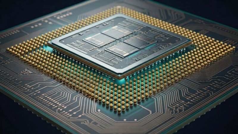
:quality(80)/p7i.vogel.de/wcms/e6/2b/e62bcec6fb21127dd59cb4d79c04381e/0132806622v1.jpeg "Next-generation packaging and testing solutions for high-density 3D power modules by JCET. (Image:JCET)")
:quality(80)/p7i.vogel.de/wcms/53/38/533875796f7f4a00cd3ff165652f3ce7/0132806622v1.jpeg "Next-generation packaging and testing solutions for high-density 3D power modules from JCET. (Image:JCET)")