Billions for Advanced PackagingChina Prepares for the Next Chip Shortage
By
Henrik Bork
| Translated by AI
5 min Reading Time
As transistors alone no longer determine the computing power of modern chips, advanced packaging is becoming a strategic bottleneck. China is responding with a new wave of investments: Between May and July 2026, projects worth around 40 billion yuan were announced.
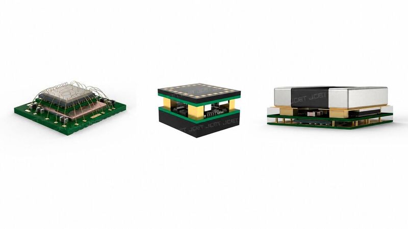
Next-generation packaging and testing solutions for high-density 3D power modules by JCET.
(Image: JCET)
China's advanced packaging industry is experiencing a new wave of capacity expansion. Between May and July 2026, nearly ten major projects were announced, with combined investments of around 40 billion yuan (nearly five billion euros / 5.5 billion USD), reports the technology portal Pandaily.
“Unlike earlier expansion cycles aimed at volume, this wave is focused on the most technically demanding segments of the packaging value chain, driven by the demand for chips for AI and high-performance computing (HPC),” writes the portal.
One reason is that Moore's Law is gradually reaching its limits. “The computing power of an AI chip no longer depends solely on transistor density. It also depends on how many layers of HBM, or high-bandwidth memory, can be stacked on top of each other,” writes the Chinese semiconductor trade publication Bandaoti Qianyan.
This stacking requires advanced packaging technologies such as the CoWoS process (Chip-on-Wafer-on-Substrate) from TSMC, the major Taiwanese contract manufacturer. Packaging now plays a role in determining the performance ceiling of a chip.
Focus on Quality
"The focus has shifted from the question of how to increase the number of transistors per unit area to how to improve the quality of the chip," the South China Morning Post quoted Zheng Li, the head of the packaging and testing company Jiangsu Changjiang Electronics Technology (JCET), as saying. He spoke at the industry conference Semicon China.
Three major projects stand out. On June 24, JCET announced the construction of a new packaging and testing factory in the Lingang Special Area in Shanghai. 7.8 billion yuan (around 950 million euros / approx. 1.08 billion USD) will be invested there in new production lines for high-density redistribution layers (RDL), ultra-fine bumping, large-format heterogeneous integration, and chiplet packaging.
There is especially demand for this in the market for AI servers, HPC systems, and graphics processors. The first phase of this project is set to become operational in the second half of 2028. "The new capacities will primarily be built around demand from the AI industry, with a particular focus on advanced packaging requirements for computing power, data storage, and power supply," writes the Chinese financial journal Zhengquan Shibao.
JCET has increased its investment budget for 2026 to around 10 billion yuan (approximately 1.2 billion euros / approx. 1.38 billion USD ), an increase of almost 18 percent compared to the previous year. According to the company, capacity utilization in the first quarter was over 80 percent. The order books are apparently full.
Further Major Investments
Two days after JCET, Forehope Electronic announced plans to invest 10.3 billion yuan (around 1.3 billion euros / approx. 1.42 billion USD) over eight years in a packaging and testing facility in Yuyao near Ningbo. Four production lines for bumping, 2.5D integration, flip-chip, and advanced wire bonding are to be established there. Target markets include AI edge processors, automotive control chips, and high-quality analog ICs.
The third major project started on July 13 in Jiading, a district of Shanghai. A subsidiary of Union Semiconductor from Hefei is investing at least 7.5 billion yuan (more than 900 million / euros approx. 1.04 billion USD) there in the "HITS" packaging process, ultra-fine bonding, high-density RDL, and large-scale heterogeneous integration, again for AI servers and HPC systems.
Part of the new packaging wave is driven by chip demand in the automotive industry. In mid-July, HKC signed a contract for a packaging and testing base worth four billion yuan (around 500 million euros / approx. 550 million USD) in Shaoxing, Zhejiang Province. After the first expansion phase, 20 million packaged chips in a 12-inch equivalent are expected to roll off the production line monthly, primarily automotive-grade components and power analog ICs.
Date: 08.12.2025
Naturally, we always handle your personal data responsibly. Any personal data we receive from you is processed in accordance with applicable data protection legislation. For detailed information please see our privacy policy.
Consent to the use of data for promotional purposes
I hereby consent to Vogel Communications Group GmbH & Co. KG, Max-Planck-Str. 7-9, 97082 Würzburg including any affiliated companies according to §§ 15 et seq. AktG (hereafter: Vogel Communications Group) using my e-mail address to send editorial newsletters. A list of all affiliated companies can be found here
Newsletter content may include all products and services of any companies mentioned above, including for example specialist journals and books, events and fairs as well as event-related products and services, print and digital media offers and services such as additional (editorial) newsletters, raffles, lead campaigns, market research both online and offline, specialist webportals and e-learning offers. In case my personal telephone number has also been collected, it may be used for offers of aforementioned products, for services of the companies mentioned above, and market research purposes.
Additionally, my consent also includes the processing of my email address and telephone number for data matching for marketing purposes with select advertising partners such as LinkedIn, Google, and Meta. For this, Vogel Communications Group may transmit said data in hashed form to the advertising partners who then use said data to determine whether I am also a member of the mentioned advertising partner portals. Vogel Communications Group uses this feature for the purposes of re-targeting (up-selling, cross-selling, and customer loyalty), generating so-called look-alike audiences for acquisition of new customers, and as basis for exclusion for on-going advertising campaigns. Further information can be found in section “data matching for marketing purposes”.
In case I access protected data on Internet portals of Vogel Communications Group including any affiliated companies according to §§ 15 et seq. AktG, I need to provide further data in order to register for the access to such content. In return for this free access to editorial content, my data may be used in accordance with this consent for the purposes stated here. This does not apply to data matching for marketing purposes.
Right of revocation
I understand that I can revoke my consent at will. My revocation does not change the lawfulness of data processing that was conducted based on my consent leading up to my revocation. One option to declare my revocation is to use the contact form found at https://contact.vogel.de. In case I no longer wish to receive certain newsletters, I have subscribed to, I can also click on the unsubscribe link included at the end of a newsletter. Further information regarding my right of revocation and the implementation of it as well as the consequences of my revocation can be found in the data protection declaration, section editorial newsletter.
Boom, also Thanks to the Automotive Industry
The new factories are usually being built right next to existing wafer plants or large automotive sites to strengthen local semiconductor supply chains, writes Pandaily. In Shaoxing, for example, UNT is already producing wafers for the automotive industry on a large scale.
A second focus is memory chips. The AI industry is struggling with the "memory wall," a new bottleneck between processor and memory. According to reports in Chinese trade media, the packaging of memory modules is therefore shifting to fan-out architectures and the integrated packaging of memory and computing chips.
Huatian Technology is currently expanding its base in Nanjing for three billion yuan (around 370 million euros / approx. 415 million USD), including packaging for HBM and testing for SSD controllers, reports Pandaily. Biwin Storage has also launched a project worth one billion yuan (around 120 million euros / approx. 138 million USD) in the southern Chinese Greater Bay Area for packaging AI memory chips. Partly, these investments are driven by the technology boycotts imposed by Washington against Beijing.
"TSMC's CoWoS capacity is stretched to its limits, the American CHIPS Act is injecting funds into domestic packaging, and Apple had to significantly raise the prices of MacBooks and iPads," writes Bandaoti Qianyan. It is evident that advanced packaging is replacing wafer manufacturing as the scarcest link in the semiconductor supply chain.
The packaging capacities of TSMC in Taiwan are now more than fully utilized, according to reports. TSMC's CoWoS utilization has been above 120 percent for some time. The share of packaging in the manufacturing costs of top-tier AI chips has risen from less than ten percent to more than 25 percent.
Investors like such "bottlenecks." While Washington's export controls deny Chinese manufacturers access to contract manufacturers like TSMC, advanced packaging in China is becoming increasingly lucrative.
The reason is technical but simple. The harder it becomes to access the finest chip feature sizes, the more important it becomes to extract more computing power from existing dies through stacking and interconnection.
Thus, advanced packaging has become part of the "chip war" between the USA and China. "The strategic goal of the United States is clear. They not only want to bring wafer manufacturing back to American soil but also rebuild a complete domestic ecosystem for advanced packaging, a segment that until recently was almost entirely dependent on Asia," writes Bandaoti Qianyan.
Intel has received $8.5 billion in direct subsidies, partly for packaging projects. TSMC is getting $6.6 billion for expansion in Arizona. Samsung has received $6.4 billion for Texas, and the packaging specialist Amkor around $407 million for a complete packaging and testing factory, also in Arizona.
The development in China mirrors these efforts in the USA. JCET, Huatian, and Tongfu Microelectronics are currently entering a "rare strategic time window," writes Bandaoti Qianyan. In China, they benefit from the fact that Chinese chip customers prefer domestic service providers for political reasons. Additional demand comes from abroad, as leading international foundries are currently focusing their resources on 3D packaging. JCET specifically aims to capture the overflowing 2.5D orders, writes Zhengquan Shibao. Rarely has geopolitics so directly contributed to a boom in an industry in China as it is currently doing for chip packaging providers.



:quality(80)/p7i.vogel.de/wcms/eb/2b/eb2bd1b8487afe577b37363cd02f16ff/0113143253v1.jpeg "In our China Market Insider, we regularly provide you with relevant information straight from China. (Image:© Eisenhans - stock.adobe.com)")
:quality(80)/p7i.vogel.de/wcms/dd/b8/ddb8edc98c49b384734ab2432b297eb5/adobestock-1913662309--irene-stock-adobe-com-ki-generiertv1.jpeg "Rotary joints are used in grippers and swivel mechanisms to allow assemblies to rotate or swivel smoothly relative to one another, even under very high loads (illustrative image). (Source: Irene - stock.adobe.com / KI-generiert)")
:quality(80)/p7i.vogel.de/wcms/d1/ef/d1ef6b6f7d4543f7999980bacccaf22b/0133499261v1.jpeg "As the growing imbalance in trade relations with China continues to widen, the EU Chamber of Commerce foresees a day when trade with China will have to be seriously reevaluated ... (Image: AI-generated)")
:quality(80)/p7i.vogel.de/wcms/fe/1f/fe1fa5ee713f94deaba963dc24c3abc5/0133299273v1.jpeg "The Flexistar enables highly flexible production of laser-welded tubes thanks to its tool-free clamping system. (Image:Because Technology, LLC)")
:quality(80)/p7i.vogel.de/wcms/60/ef/60ef4f07e4829b2c2929befc0f353c58/0133511729v1.jpeg "Humanoid robots can match human performance in certain tasks. (Image:Gemini / AI-generated)")
:quality(80)/p7i.vogel.de/wcms/2e/99/2e99726b522e4b35b690e25eb6a42643/0133463991v1.jpeg "Robotics: In AMR applications, connection technology must reliably transmit power, signals, and data despite vibration and shock loads—in very confined spaces and in a way that allows for regular maintenance. (Image:Hyperever)")
:quality(80)/p7i.vogel.de/wcms/d0/18/d01801e3d5dbd7bc9d0b4f60408b630c/0133468429v1.jpeg "Quality requirements for film packaging are on the rise. At the same time, many companies are turning to recyclable film materials, which, however, have their own challenges. Fraunhofer researchers have therefore developed a fast system that detects problems in real time. (Image:Fraunhofer IKTS)")
:quality(80)/p7i.vogel.de/wcms/b1/06/b106cf44923ce39565c3264982fd20eb/0133414574v1.jpeg "Robots Build Robots: At the new Ubtech factory, automated systems even handle parts of the material supply and logistics for the production of humanoid robots. (Image:Ubtech)")
:quality(80)/p7i.vogel.de/wcms/c0/52/c052f405eb55fc3d08c4837e77206fc0/adobestock-2021845957--aucartstudio-stock-adobe-com-ki-generiertv1.jpeg "An innovation from China to combat extreme summer heat: A novel coating lowers temperatures. (Source: © AucArtStudio – stock.adobe.com_AI-generated)")
:quality(80)/p7i.vogel.de/wcms/66/a7/66a7b78159caeacce57136529688799f/0133503398v1.jpeg "Sunlight Makes Stone! These stone blocks weren't made the traditional way. Instead, they were additively manufactured from sand using a laser. In the future, however, the laser is set to be replaced by concentrated sunlight—if the startup Addisol is successful... (Image:Addisol / F. Fiedler)")
:quality(80)/p7i.vogel.de/wcms/72/b9/72b995c2c8d812c5e2115cbef31e035a/0133462727v1.jpeg "Eggl manufactures center hoods that are precisely tailored to each cooking island—whether standard size or custom shape. They are made entirely of stainless steel and are individually customized in terms of size and filter arrangement. (Image:SPI)")
:quality(80)/p7i.vogel.de/wcms/13/5d/135dfae6229ceaf5c55467a43e8f7257/adobestock-1879961393--ardi-stock-adobe-com-ki-generiertv1.jpeg "Annoying chatterboxes or awkward silences in response to questions—a moderator should specifically prepare for difficult situations in order to navigate them effectively. (Image:ardi - stock.adobe.com_AI-generated)")
:quality(80)/p7i.vogel.de/wcms/3e/2f/3e2f1ec6c4e1a24eac32957acebd0901/0133601693v1.jpeg "From the boule (bottom) to the wafer to the chip (on top of the boule). Transistors are used as switches in power electronics. (Image:Bosch)")
:quality(80)/p7i.vogel.de/wcms/8f/99/8f9956e7dce99d1b28c27fb1c30ea236/04-dsc-2230v1.jpeg "Bosch is cutting jobs in Nuremberg. (Source: Bosch)")
:quality(80)/p7i.vogel.de/wcms/aa/a2/aaa2c6dd2daa24b485cddbf9297590c0/0133467318v1.jpeg "Battery Monitoring: Battery monitoring using electrochemical impedance spectroscopy offers several advantages. (Image:TI)")
:quality(80)/p7i.vogel.de/wcms/39/b2/39b21bf03be1683831862239a369987c/0133469638v1.jpeg "Data from autonomous vehicles and robots operating autonomously is in high demand, and Ruqi wants to capitalize on this. (Image:Ruqi Mobility)")
:quality(80)/p7i.vogel.de/wcms/28/28/2828c5261714321afb0bab67bf771823/0133353387v1.jpeg "The 130-meter-long China Zorrilla draws its power from a battery system with a capacity of more than 40 MWh. Eight electric motors drive an equal number of water jets. (Image:Incat Australia Pty Ltd)")
:quality(80)/p7i.vogel.de/wcms/48/15/4815da27c45973ca629a99b375ac3aef/0133509585v1.jpeg "Ventuno Q RoadTest: Designed to help the Element14 community gain practical insights from real-world tests using the Ventuno Q. (Image:Farnell/Element14)")
:quality(80)/p7i.vogel.de/wcms/17/2b/172bd132f9febdfcbcedba292ad0504d/aufmacherv1.jpeg "Micro-Epsilon offers a wide range of IO-Link-compatible sensors. (Source: Micro-Epsilon Messtechnik GmbH & Co. KG)")
:quality(80)/p7i.vogel.de/wcms/ca/b4/cab46fd26d19d6a2febca032048200b6/0133471827v1.jpeg "Photonics SDK for C and Python: Computational operations are now abstracted as standard mathematical functions. (Image:Q.ANT)")
:quality(80)/p7i.vogel.de/wcms/83/a9/83a9493ad202f37e188f3323c56aa2c6/0132672260v1.jpeg "After Moore's Law: Packaging is becoming the most important driver for semiconductor technology. (Image: ©Svitlana - stock.adobe.com)")
:quality(80)/p7i.vogel.de/wcms/1a/bf/1abf6e3b862a9ba71914b9ef7dce0ca4/0132761112v1.jpeg "Semiconductor scaling: TSMC's roadmap reveals a fundamental shift. Development is no longer solely determined by transistor density, but scaling is moving from the individual chip to the system level. (Image:TSMC)")
:quality(80)/p7i.vogel.de/wcms/53/38/533875796f7f4a00cd3ff165652f3ce7/0132806622v1.jpeg "Next-generation packaging and testing solutions for high-density 3D power modules from JCET. (Image:JCET)")
:quality(80)/p7i.vogel.de/wcms/57/d2/57d2b75d884c18866b46e776126fb46b/org-blobs-user-response-file-output-dac07b02-0e97-4452-9a3a-26528da583b3-file-1787126178766-jpgv1.jpeg "The memory manufacturer CXMT has had an extremely successful IPO. Among the investors are several car manufacturers. (Image:KI-generiert)")