Voids formed during the epitaxial filling of SiC trenches reduce the breakdown voltage. However, eliminating them can increase the on-resistance. A simulation study examines how this trade-off can be resolved—and why the position of a defect is critical.
In SiC superjunction devices, the trench geometry and epitaxial filling influence the trade-off between breakdown voltage and on-resistance.
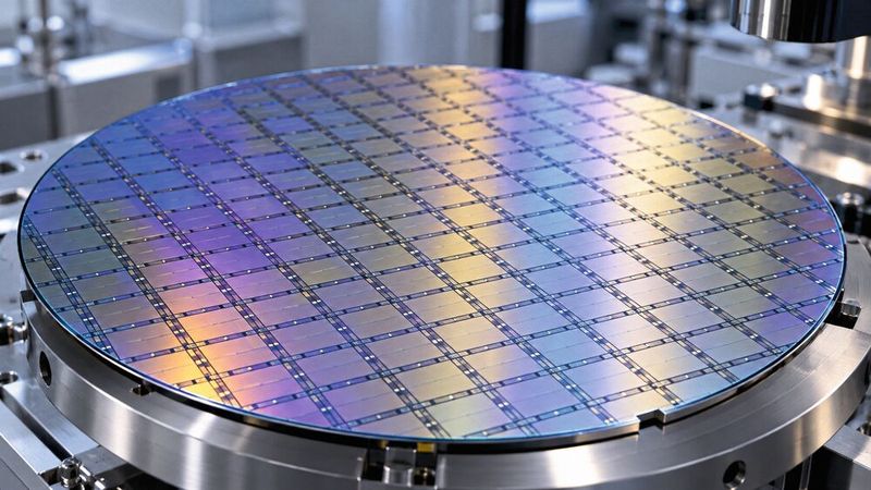
(Image: Dall-E / AI-generated)
In SiC superjunction devices, narrow, nearly vertical columns offer a favorable compromise between breakdown voltage and specific on-resistance RDS(on),sp, i.e., the resistance multiplied by the active area in the conducting state. However, their fabrication is challenging: When deep trenches are filled epitaxially, the opening can close before the underlying space is completely filled with semiconductor material. This leaves behind a void that alters the charge distribution and the electric field.
Wider trenches with steeper sidewalls make it easier to fill them without leaving voids. However, this geometry is not necessarily more advantageous from an electrical standpoint. It is precisely this relationship that Bailing Zhou’s team investigates in the study “Simulation study of void impact in trench-filling-epitaxy-based 4H-SiC semi-superjunction Schottky rectifiers”, published in Power Electronic Devices and Components. The authors combine device simulations with numerical optimization and compare two approaches: avoiding voids through geometry or specifically accounting for them during the design process.
Charge Compensation Meets Manufacturing Limits
Superjunction structures utilize adjacent p- and n-doped columns whose space charges largely compensate each other in reverse-bias operation. This allows the current-carrying n-region to be more heavily doped than would be possible with a conventional unipolar drift region having the same breakdown voltage. The electrical resistance decreases. In the Schottky diodes made of 4H silicon carbide examined in this study, the charge compensation structure extends only over a portion of the drift region. Below the columns, there is also a weakly n-doped layer. The study uses the term “semi-superjunction” (SSJ) to describe this configuration.
The study considers two methods for fabricating the columns. In epitaxial trench filling with p-doped SiC (P-type trench filling, PTF), trenches in an n-doped region are filled with p-doped SiC. In the case of n-doped SiC trench filling (N-type trench filling, NTF), the n-pillar is formed by filling a trench in a p-doped region. This difference determines whether a void is located in the charge-compensating p-column or directly in the current-carrying n-region.
The authors investigate trench widths of 1.5 and 3.0 µm, as well as trench sidewall inclinations relative to the vertical of 2°, 5°, and 8°, omitting any geometrically unsuitable combinations for NTF. The cavity shapes are derived from experimental cross-sectional images and incorporated into two-dimensional models for physical device simulation (Technology Computer-Aided Design, TCAD). The electrical parameters are derived from simulations using Synopsys Sentaurus. A mathematical Ersatz model (response surface model) based on these results describes how the electrical parameters depend on dopant concentrations and accelerates the optimization process. Selected designs are then re-evaluated using TCAD.
A Defect in the P-Column Can Be Partially Compensated for
If the void is located in the p-column, part of the semiconductor volume is missing there, and thus the charge of ionized acceptors available for compensation. With the doping remaining unchanged, the ratio between the p- and n-columns becomes unbalanced. The breakdown voltage decreases.
The narrow PTF structure with a 2° sidewall angle illustrates just how significant this effect is: Without a cavity, it reaches a breakdown voltage of 1,470 V in the simulation. With a cavity and unchanged doping, the breakdown voltage remains at 1,173 V. If the p-doping is adjusted to account for the reduced semiconductor volume, the value increases to 1,324 V. The specific on-resistance remains at around 0.22 mΩ·cm² in the study’s table.
The adjustment restores the charge balance integrated over the entire column region. However, it does not eliminate the local disturbance along the column. Therefore, a loss of 146 V remains compared to the cavity-free reference. For wide PTF trenches, this remaining loss is significantly smaller: The study cites 15 V at 2° and 12 V at 5°.
The Current Path is Further Restricted in the N-Pillar
In NTF structures, the void also affects the conductive cross-section of the n-column. In addition to the breakdown voltage, this causes the on-resistance to deteriorate. For the narrow 2° structure, the breakdown voltage drops from 1,510 to 1,306 V after the nominal charge balance is restored. At the same time, according to the authors, the specific on-resistance increases by about 25%.
For the NTF designs examined, this study therefore favors a wide, inclined structure filled without voids. For PTF, on the other hand, even a narrow, nearly vertical trench with a void remains a possible design option: its low resistance can offset some of the disadvantage in terms of breakdown voltage. Which variant is suitable thus also depends on the required blocking capability.
Date: 08.12.2025
Naturally, we always handle your personal data responsibly. Any personal data we receive from you is processed in accordance with applicable data protection legislation. For detailed information please see our privacy policy.
Consent to the use of data for promotional purposes
I hereby consent to Vogel Communications Group GmbH & Co. KG, Max-Planck-Str. 7-9, 97082 Würzburg including any affiliated companies according to §§ 15 et seq. AktG (hereafter: Vogel Communications Group) using my e-mail address to send editorial newsletters. A list of all affiliated companies can be found here
Newsletter content may include all products and services of any companies mentioned above, including for example specialist journals and books, events and fairs as well as event-related products and services, print and digital media offers and services such as additional (editorial) newsletters, raffles, lead campaigns, market research both online and offline, specialist webportals and e-learning offers. In case my personal telephone number has also been collected, it may be used for offers of aforementioned products, for services of the companies mentioned above, and market research purposes.
Additionally, my consent also includes the processing of my email address and telephone number for data matching for marketing purposes with select advertising partners such as LinkedIn, Google, and Meta. For this, Vogel Communications Group may transmit said data in hashed form to the advertising partners who then use said data to determine whether I am also a member of the mentioned advertising partner portals. Vogel Communications Group uses this feature for the purposes of re-targeting (up-selling, cross-selling, and customer loyalty), generating so-called look-alike audiences for acquisition of new customers, and as basis for exclusion for on-going advertising campaigns. Further information can be found in section “data matching for marketing purposes”.
In case I access protected data on Internet portals of Vogel Communications Group including any affiliated companies according to §§ 15 et seq. AktG, I need to provide further data in order to register for the access to such content. In return for this free access to editorial content, my data may be used in accordance with this consent for the purposes stated here. This does not apply to data matching for marketing purposes.
Right of revocation
I understand that I can revoke my consent at will. My revocation does not change the lawfulness of data processing that was conducted based on my consent leading up to my revocation. One option to declare my revocation is to use the contact form found at https://contact.vogel.de. In case I no longer wish to receive certain newsletters, I have subscribed to, I can also click on the unsubscribe link included at the end of a newsletter. Further information regarding my right of revocation and the implementation of it as well as the consequences of my revocation can be found in the data protection declaration, section editorial newsletter.
Smaller Cavities are not Necessarily Less Harmful
Another finding is relevant to process development, as the cavity area alone does not adequately describe the electrical effect. In the narrow PTF structures, it decreases as the sidewall angle increases. Nevertheless, after the global charge balance is restored, the 8° variant causes a greater loss in breakdown voltage than the 2° variant: 254 V instead of 146 V.
As the angle changes, the shape, position, and distance of the cavity from the column flank change simultaneously. These parameters influence local charge compensation and field distribution. A process that creates smaller cavities does not necessarily result in components with more favorable electrical properties. For the evaluation of cross-sectional images, this implies that defect geometry and component structure should be considered together.
A Broader Doping Window Requires a Clear Reference
The simulations also show lower sensitivity to certain doping variations. The doping window reported in the paper is, in some cases, significantly widened by voids. The authors define the window as the range in which the breakdown voltage reaches at least 80% of the value at nominal charge balance.
This relative reference is crucial for interpretation. If the breakdown voltage of the reference state decreases, the 80% threshold is also lower. A wider window therefore does not necessarily indicate a higher production yield if the absolute reverse voltage requirement remains unchanged. To determine this, the permissible doping range would need to be evaluated against this specific requirement.
The practical value of this work lies primarily in the joint optimization of the process and the component. It quantifies the electrical drawbacks caused by a void and the potential drawbacks that can arise if the trench geometry is designed solely to avoid it. From this, candidates for further manufacturing trials and electrical tests can be identified.
Bailing Zhou: „Simulation study of void impact in trench-filling-epitaxy-based 4H-SiC semi-superjunction schottky rectifiers“, Power Electronic Devices and Components, 2026, Artikel 100153.



:quality(80)/p7i.vogel.de/wcms/14/43/1443db59695f7eed2a338d16d03a6257/26-09-30-st-ber-ab-hunger-games-bild-1v1.jpeg "For “The Hunger Games: On Stage,” drive systems lift and move grandstand sections with a dynamic load of up to 26 metric tons—each section can accommodate up to 112 spectators. (Source: Troubadour at the Canary Wharf Theatre)")
:quality(80)/p7i.vogel.de/wcms/5f/96/5f9606264f35f5979529286a887bbccf/0133859498v1.jpeg "Trumpf Expands Its Portfolio for 2D Laser Cutting (Image:TRUMPF GMBH + CO. KG)")
:quality(80)/p7i.vogel.de/wcms/6d/76/6d7682de33991e539956ed72f7d246a3/vibro-cutv1.jpeg "Hybrid machining uses ultrasonic and oscillation technologies to support traditional machining processes. (Source: VibroCut)")
:quality(80)/p7i.vogel.de/wcms/ed/78/ed786ed6b280ff6c692908f01f715e3d/0113143253v1.jpeg "In our China Market Insider, we regularly provide you with relevant information straight from China. (Image:© Eisenhans - stock.adobe.com)")
:quality(80)/p7i.vogel.de/wcms/a8/0d/a80d9eb978dd47dbd8f390181a039bfc/adobestock-2081783940--design-store-stock-adobe-com-ki-generiertv1.jpeg "We’re showcasing five of the latest innovations for virtual commissioning—from AI copilots and smart browser tools to deep PLC integration. (Source: © Design Store – stock.adobe.com_AI-generated)")
:quality(80)/p7i.vogel.de/wcms/87/88/8788e0b7fd98cca21a9c370ed0f0aa18/0133859688v1.jpeg "The software newly developed at Fraunhofer IWU helps employees reliably
identify parts that do not meet quality requirements. (Image:Fraunhofer IWU)")
:quality(80)/p7i.vogel.de/wcms/4b/7c/4b7c11f510878f154012d04c18a7c3cc/0133798118v1.jpeg "RobCo Becomes a Unicorn: The Munich-based robotics company has reached a valuation of more than one billion U.S. dollars and is driving the next generation of autonomous industrial robotics with Alfie. (Image:RobCo)")
:quality(80)/p7i.vogel.de/wcms/c8/a9/c8a96d5841d508c9e9c609c64168cbaa/0133758997v1.jpeg "Hospital Robotics: Neura Robotics' autonomous healthcare platform is designed to independently transport empty hospital beds between wards and floors. (Image:Neura Robotics)")
:quality(80)/p7i.vogel.de/wcms/8a/c8/8ac8eb7fc2b70f4b72771548e2e2e520/epfl-motor-3v1.jpeg "FiberMotor has a diameter of 1 to 3 mm and consists of two concentric hollow fibers. Each fiber is wrapped in tightly insulated copper wire electrodes that are only slightly thicker than a human hair. (Source: EPFL)")
:quality(80)/p7i.vogel.de/wcms/a7/8a/a78a582a42a96aaaff38bd6b8f97a015/vishal-lal-mit-kernuhrv1.jpeg "It's ticking: Researchers have stabilized the first atomic clock. (Source: PTB)")
:quality(80)/p7i.vogel.de/wcms/36/f9/36f96a206fc408c9a632ce849de1f7fa/newsimage428299v1.jpeg "Polystyrene is used in protective packaging for televisions and electronic devices, in decorative moldings and baseboards for interior home construction, and even in Petri dishes. (Source: Hereon/Marcel Schwickerath)")
:quality(80)/p7i.vogel.de/wcms/90/30/90300137452b00d22f95113eff065ac3/fliehkraftkupplungen-und-bremsen-montage-centrifugal-clutches-and-brakes-assembly-1v1.jpeg "Installation: Centrifugal clutches should always be precisely matched to the machine. (Source: Amsbeck Machine Technology)")
:quality(80)/p7i.vogel.de/wcms/50/23/5023ffaefac8f9a47286b368143b88eb/0133801078v1.jpeg "Life isn't exactly a walk in the park for Porsche right now. And now Porsche management is saying that next year will be even worse. Read here to find out why that's supposed to be the case... (Image: Porsche)")
:quality(80)/p7i.vogel.de/wcms/2f/ab/2fabf62cdd2f57cb279e00931c91c869/0133794991v1.jpeg "The Atto 2 SUV is one of BYD's most popular plug-in hybrids. (Image:BYD)")
:quality(80)/p7i.vogel.de/wcms/e9/6e/e96e34d467ca1017f2a689275ae07302/0133815122v1.jpeg "Porsche CEO Leiters has shared new information about the company's model plans. (Image:Porsche)")
:quality(80)/p7i.vogel.de/wcms/0a/50/0a50938be0b598b36efc4e5457ed56dd/forvia-siege-zen-massage-16-9-06v1.jpeg "Seat with massage function by Forvia. (Source: Forvia)")
:quality(80)/p7i.vogel.de/wcms/4c/59/4c59ffe8ca03e2b17250ff39ac57d3a7/0133803993v1.jpeg "Making greater use of plant-based proteins would be beneficial, but they can contain bitter peptides. However, with a new AI, it is now possible to predict their taste in order to specifically produce the right peptides. The image shows the bitter taste receptor pocket with a bound tripeptide (yellowish). (Image:F. Bößl / Leibniz-LSB)")
:quality(80)/p7i.vogel.de/wcms/c4/11/c41181159e23eafeffe6c06b9e496859/0133788141v1.jpeg "Simplicity AI SDK: Silicon Labs has released its AI-powered developer SDK as a public beta, thereby integrating AI assistants into the embedded development process. (Image:Silicon Labs)")
:quality(80)/p7i.vogel.de/wcms/f5/22/f5221ac972f35e5befc24a040ce7b19e/0133841330v1.jpeg "Chip-on-Cell technology: The Dukosis DK8102 measurement chip measures cell voltage and temperature directly at the battery cell and transmits the data to the battery management system. (Image:Dukosi)")
:quality(80)/p7i.vogel.de/wcms/97/5e/975e764c44174e6091b169f1d4682dbf/0133820837v1.jpeg "In SiC superjunction devices, the trench geometry and epitaxial filling influence the trade-off between breakdown voltage and on-resistance. (Image:Dall-E / AI-generated)")
:fill(fff,0)/images.vogel.de/vogelonline/companyimg/76800/76895/65.jpg "FAULHABER_120mm.jpg ()")
:quality(80)/p7i.vogel.de/wcms/2a/2f/2a2fc1bb2a6941d1e5c795c047c969ce/0132945015v1.jpeg "Developers at the lab workplace: For WBG-based power converters and highly dynamic loads, precise efficiency and loss analysis require the time-synchronized acquisition of electrical, transient, and thermal parameters. (Image:Yokogawa)")
:quality(80)/p7i.vogel.de/wcms/3e/2f/3e2f1ec6c4e1a24eac32957acebd0901/0133601693v1.jpeg "From the boule (bottom) to the wafer to the chip (on top of the boule). Transistors are used as switches in power electronics. (Image:Bosch)")
:quality(80)/p7i.vogel.de/wcms/b7/e2/b7e2324dedc6c9c96d5f265f06aa409e/0132928076v1.jpeg "Compact and standardized: CubeSats enable cost-effective space missions and increasingly serve as a platform for testing new technologies – from sensors and communication to innovative energy supply systems. (Image:City Labs, Inc.)")