In wafer dicing, not only are more precise laser processes important but also intelligent process monitoring. Researchers at Chiba University have now presented an interesting approach: they measure the recoil force generated during material removal. This could make laser dicing a self-monitoring manufacturing process.
Laser Dicing: From the recoil force of the laser pulse upon impact on the semiconductor, a reproducible process signal can be derived in real time, enabling automated control of wafer dicing.
The separation of semiconductor chips from a processed wafer is a crucial step in the backend of semiconductor manufacturing. In this process, the wafer is cut into so-called dies using a diamond saw, which form the actual semiconductor components. Wafer dicing today significantly determines the yield, reliability, and cost-effectiveness of a process. At the same time, wafers are becoming thinner, and mechanical reserves are decreasing. As a result, traditional diamond sawing methods are reaching their limits.
The industry is currently developing several methods in parallel. In addition to traditional laser ablation cutting, stealth dicing, waterjet-guided laser dicing, and hybrid processes are gaining importance. The goal of all developments is to further reduce material removal, avoid microcracks, and simultaneously significantly increase throughput.
Gallery
Laser cutting, where individual chips are separated using focused laser pulses on the semiconductor wafer, is increasingly preferred as sensitive, more ductile materials can be processed with minimal mechanical stress. However, achieving an adequate yield requires precise process control.
With increasing process speed, however, the processing state, i.e., the penetration depth of the laser pulse, can only be monitored to a limited extent during laser operation. To this day, many systems rely on optical inspection systems or downstream quality controls. This is precisely where the research of Chiba University comes into play.
Evaluate Process Signals in Real Time
The approach of the Japanese scientists led by Professor Hirofumi Hidai from the Graduate School of Engineering at Chiba University focuses on recoil force. This is a reaction force that is generated on the surface of a material when it is rapidly heated and vaporized by a laser pulse. According to the law of conservation of momentum, an equal and opposite force acts on the material in this process.
The Japanese use the recoil force as a direct process control signal for laser dicing. Instead of cameras or confocal sensors, a piezoelectric force sensor exclusively registers the counterforce generated during material removal. This allows conclusions to be drawn about the actual machining process.
The results of the study will be published on November 1, 2026, in Volume 203 of the journal "Optics and Laser Technology."
Recoil force as an in-situ process signal
Chiba University demonstrates for the first time that the recoil force generated during laser dicing can be used as an in-situ process signal. It correlates with the processing depth, detects wafer breakthrough, and thus enables continuous monitoring of laser dicing without additional optical sensors. The authors view this as a promising approach for future closed-loop controls in semiconductor manufacturing.
That's why this is important: The boom in generative AI is increasing the demand for high-performance processors and HBM memory. At the same time, nearly all leading semiconductor manufacturers are adopting chiplet architectures and advanced packaging. As a result, the number of high-value dies per wafer, and thus the economic value of each individual dicing step, is rising. Process monitoring is becoming a productivity factor.
For the experiments, the researchers used a nanosecond-pulse Nd-YAG laser with a wavelength of 1064 nm and a pulse duration of 25 ns. To measure the recoil force, the scientists utilized a piezoelectric force sensor. Simultaneously, the actual processing depth was measured confocally. This allowed the measured recoil force to be directly compared with the actual material removal.
The results show an almost linear relationship between pulse energy and recoil force. Above a pulse energy of approximately 3 mJ, plasma effects limit further material removal. The recoil force remains a reproducible process signal and provides real-time information about the process.
Determine Machining Depth in Real Time
During multi-pulse machining, the recoil force continuously decreases. The cause is the increasing defocusing of the laser beam with growing drilling depth. The authors derived a mathematical model from this, which calculates the machining depth directly from the measured force.
With an average relative deviation of around 24%, the method does not yet replace high-precision measurement technology. However, the depth information is generated directly during the machining process. And this is achieved without a camera, without additional measurement optics, and independently of the contour (deep or narrow) of the cutting grooves.
Clearly Detect Wafer Cutting
Particularly interesting is the behavior just before the wafer is completely cut through. The course of the recoil force changes significantly at this point. This allows the exact moment when a wafer is fully cut to be determined without the need for visual inspection of the sample.
Date: 08.12.2025
Naturally, we always handle your personal data responsibly. Any personal data we receive from you is processed in accordance with applicable data protection legislation. For detailed information please see our privacy policy.
Consent to the use of data for promotional purposes
I hereby consent to Vogel Communications Group GmbH & Co. KG, Max-Planck-Str. 7-9, 97082 Würzburg including any affiliated companies according to §§ 15 et seq. AktG (hereafter: Vogel Communications Group) using my e-mail address to send editorial newsletters. A list of all affiliated companies can be found here
Newsletter content may include all products and services of any companies mentioned above, including for example specialist journals and books, events and fairs as well as event-related products and services, print and digital media offers and services such as additional (editorial) newsletters, raffles, lead campaigns, market research both online and offline, specialist webportals and e-learning offers. In case my personal telephone number has also been collected, it may be used for offers of aforementioned products, for services of the companies mentioned above, and market research purposes.
Additionally, my consent also includes the processing of my email address and telephone number for data matching for marketing purposes with select advertising partners such as LinkedIn, Google, and Meta. For this, Vogel Communications Group may transmit said data in hashed form to the advertising partners who then use said data to determine whether I am also a member of the mentioned advertising partner portals. Vogel Communications Group uses this feature for the purposes of re-targeting (up-selling, cross-selling, and customer loyalty), generating so-called look-alike audiences for acquisition of new customers, and as basis for exclusion for on-going advertising campaigns. Further information can be found in section “data matching for marketing purposes”.
In case I access protected data on Internet portals of Vogel Communications Group including any affiliated companies according to §§ 15 et seq. AktG, I need to provide further data in order to register for the access to such content. In return for this free access to editorial content, my data may be used in accordance with this consent for the purposes stated here. This does not apply to data matching for marketing purposes.
Right of revocation
I understand that I can revoke my consent at will. My revocation does not change the lawfulness of data processing that was conducted based on my consent leading up to my revocation. One option to declare my revocation is to use the contact form found at https://contact.vogel.de. In case I no longer wish to receive certain newsletters, I have subscribed to, I can also click on the unsubscribe link included at the end of a newsletter. Further information regarding my right of revocation and the implementation of it as well as the consequences of my revocation can be found in the data protection declaration, section editorial newsletter.
Especially in highly automated production lines, this could reduce the number of unnecessary laser pulses. At the same time, the risk of damaging dicing films or subsequent substrates decreases.
A Step Towards the Semiconductor Manufacturing of the Future
The true significance of the work lies in its potential for real-time process monitoring. In semiconductor manufacturing, processes are not only monitored but are also intended to be automatically adjusted. Closed-loop systems adapt laser power, focal position, or feed rate during machining to match the actual process state. This requires robust sensor signals that are directly obtained from the manufacturing process.
The recoil force arises directly from the interaction between the laser and the material, making it significantly closer to the actual process than downstream image analysis.
In the future, force measurement could be combined with AI-supported control algorithms. These would detect deviations early and automatically optimize laser parameters. This could not only reduce waste but also lower energy consumption and increase process stability.
Industrial Series Production Not Yet Foreseeable
Several challenges remain before industrial series application is feasible. The researchers particularly highlight the dynamics of the measurement system, higher pulse frequencies, and the influence of scanner movements as open fields of development. Additionally, the transfer to high-speed systems with repetition rates of several kilohertz still needs to be investigated.
Nevertheless, the research project already points to a direction in which modern laser processes could develop: away from open machining workflows and toward self-monitoring manufacturing systems that continuously assess their own process state.
Conclusion: Recoil Force as a Means of intelligent Process monitoring
The presented recoil force measurement is far more than an academic idea. It addresses one of the central topics of semiconductor manufacturing: intelligent process monitoring in the era of advanced packaging, chiplets, and AI accelerators. While traditional sensor systems observe the process externally, the new approach utilizes a signal that arises directly from the laser-material interaction.
If the process can be further developed for industrial series production, it could lead to a new sensor type for smart fabs—robust, cost-effective, and directly integrated into the manufacturing process. This would make laser dicing a decisive step towards autonomous semiconductor manufacturing.



:quality(80)/p7i.vogel.de/wcms/68/a5/68a5ce0896756c1dcf48dbeceefafbd3/0132300990v1.jpeg "Christoph Geigges is President and CEO of Walter AG. Headquartered in Tübingen (Germany), the company is one of the world’s leading suppliers of precision tools for metalworking. Under Geigges’ leadership, this long-established company is increasingly transforming itself from a tool manufacturer into an engineering partner that supports the entire manufacturing process. (Image: Walter AG)")
:quality(80)/p7i.vogel.de/wcms/3e/7c/3e7c26f44c68545fc7318597b6b65903/0133649650v1.jpeg "The flexible Heller circular storage system can store and process pallets measuring both 630 millimeters by 630 millimeters and 800 millimeters by 800 millimeters—even in mixed-mode operation. This makes the entire production line particularly flexible. (Image:Brighter)")
:quality(80)/p7i.vogel.de/wcms/16/29/162983885950ec1df27ab441bfe88613/0133132549v1.jpeg "Bernd Hermeler is the CEO of Cemecon AG. He studied mechanical engineering at RWTH Aachen University (Germany)—the very university from which the company emerged as a spin-off 40 years ago. Today, Hermeler is responsible for the global strategy of the coating specialist, which, with branches in Europe, the U.S., China, Japan, and India, is considered the global technology leader in the coating of cutting tools. (Image: Cemecon AG)")
:quality(80)/p7i.vogel.de/wcms/af/81/af81b53cb4926dcadc20ba369a29d412/0132695968v1.jpeg "International venture capital is increasingly flowing into the machining industry. Here are the players that entrepreneurs and CEOs should keep an eye on right now. (Image: ©NDABCREATIVITY - stock.adobe.com)")
:quality(80)/p7i.vogel.de/wcms/88/dc/88dc38a1a0b5e016192ab83b0850fbd0/0133514708v1.jpeg "Scalable data sovereignty is the foundation for the transition from computationally intensive AI processing and growing data streams to sustainable, energy-efficient storage systems. (Image:Gemini / AI-generated)")
:quality(80)/p7i.vogel.de/wcms/1c/ef/1cef66e13c5cc02c5731fefcc99c00d2/0133697754v1.jpeg "Embodied AI in Industry: FMC³ Robotics combines AI-based perception and adaptation with traditional robot control to prepare robots for use in industrial manufacturing. (Image:FMC³/processed by AI)")
:quality(80)/p7i.vogel.de/wcms/db/ca/dbcae78eb8853b53fe122832fe3b2cba/0132914918v1.jpeg "Robotics in Flexible Manufacturing: As connectivity increases, so do the requirements for functional safety. (Image: Delta Electronics)")
:quality(80)/p7i.vogel.de/wcms/ea/18/ea18e84aed24bbe1c91937f30c2f7301/image1v1.jpeg "Kassow Robots' new product portfolio now includes seven 7-axis cobots. (Image: Kassow Robots (Image:)")
:quality(80)/p7i.vogel.de/wcms/90/30/90300137452b00d22f95113eff065ac3/fliehkraftkupplungen-und-bremsen-montage-centrifugal-clutches-and-brakes-assembly-1v1.jpeg "Installation: Centrifugal clutches should always be precisely matched to the machine. (Source: Amsbeck Machine Technology)")
:quality(80)/p7i.vogel.de/wcms/93/84/9384230e840a99a2015fdd3e0af11e2b/newsimage428236v1.jpeg "The crutch replicates the natural, biomechanical movement pattern of the human body. (Source: Leon Kast)")
:quality(80)/p7i.vogel.de/wcms/5b/a2/5ba21b3e5fcdd91f6bfe806f745ea723/isc-physioink-bild-3v1.jpeg "In the PhysioINK project, Fraunhofer researchers are developing bio-printing inks from the most common tissue proteins. Under the microscope, the living tissue cells (fibroblasts) are visible in the printed lattice structure: blue represents the cell nucleus, and green represents the cytoskeleton. (Source: Tobias Weigel/Fraunhofer ISC)")
:quality(80)/p7i.vogel.de/wcms/9c/16/9c16e4aa02594fe4bf82ead736562b07/directhop1-scaledv1.jpeg "Light as a feather, but without feathers: The University of Washington's robot, which weighs just one gram, uses a bionic direct-drive system to catapult itself into the air with centimeter-level precision. (Source: Mark Stone/University of Washington)")
:quality(80)/p7i.vogel.de/wcms/0a/50/0a50938be0b598b36efc4e5457ed56dd/forvia-siege-zen-massage-16-9-06v1.jpeg "Seat with massage function by Forvia. (Source: Forvia)")
:quality(80)/p7i.vogel.de/wcms/99/61/9961719acb89bc87fdecb1bba140481c/0133725593v1.jpeg "Ultrason (PSU, PESU, PPSU) is suitable for E&E components used in electric mobility or AI infrastructure, such as connectors for fiber-optic cables. (Image:BASF)")
:quality(80)/p7i.vogel.de/wcms/42/9b/429badd88cd4a74edb6491d10310349c/wayve-london-05v1.jpeg "Wayve is developing an AI software stack for automated driving. It appears that the Volkswagen Group has now opted for this technology. (Source: Wayve)")
:quality(80)/p7i.vogel.de/wcms/14/9f/149f934f87e5418748fa41a611586a4f/rawdon-gloverv1.jpeg "Rowdon Glover, Managing Director of Jaguar: “We are willing to accept polarization.” (Image:JLR)")
:quality(80)/p7i.vogel.de/wcms/36/f0/36f0472d20227013871aa790f4d48ac6/0133726018v1.jpeg "Ion beams can ablate, coat, or smooth surfaces down to the atomic level. Such processes are used, among other things, in optical chips, precision optics, and superconducting materials. (Image:AI-generated)")
:quality(80)/p7i.vogel.de/wcms/1f/47/1f47da6ee12c38a745eb478a04157a65/0133726100v1.jpeg "The schematic diagram shows the structure of a 3D NAND memory device with memory cells stacked on top of one another and vertical connections for high storage density. (Image:Dall-E / AI-generated)")
:quality(80)/p7i.vogel.de/wcms/70/59/7059db055d4eeb8dea752651a071f360/geralt-handshake-4608297v1.jpeg "The deal between Schneider Electric and PTC is intended to create end-to-end data flows for the industry. (Source: )")
:quality(80)/p7i.vogel.de/wcms/67/3d/673d8f6f14bd030b53b61800a0aeb06d/0133548286v1.jpeg "Overview: If even a single critical component is missing, the entire production process can come to a standstill. Proactive procurement is intended to mitigate such bottlenecks early on. (Image:Dall-E / AI-generated)")
:fill(fff,0)/images.vogel.de/vogelonline/companyimg/76800/76895/65.jpg "FAULHABER_120mm.jpg ()")
:fill(fff,0)/p7i.vogel.de/companies/69/de/69de1b7403b0d/simtos-logo.jpeg "simtos-logo (SIMTOS)")
:quality(80)/p7i.vogel.de/wcms/8d/fd/8dfd7896bf26a5148df207aee1ba31b3/0132742025v1.jpeg "(Image: Ciba University)")
:quality(80)/p7i.vogel.de/wcms/ac/32/ac327c1e4125ecebf49f2df9ab6b242a/0132741778v1.jpeg "Image 1: Schematic representation of the experimental setup for measuring the recoil force. (a) Overall view. (b) Setup of the recoil measuring unit (BS: beam splitter; HWP: half-wave plate; PBS: polarizing beam splitter; ND filter: neutral density filter; PD: photodetector). (c) Coordinate definition at the processing point.(Image: Ciba University / CC BY-SA 4.0)")
:quality(80)/p7i.vogel.de/wcms/b7/7b/b77b10a7628be04473298b69d4234b99/0132741781v1.jpeg "Image 3: Relationship between the number of laser pulses and the recoil force.(Image: Ciba University / CC BY-SA 4.0)")
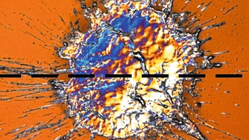
:quality(80)/p7i.vogel.de/wcms/90/b6/90b645208ce36c4a0c90e614303b300d/0132741784v1.jpeg "Image 2: Examination of the irradiated silicon surface. (a) Differential interference contrast microscopy image. (b) Cross-sectional profile along the dashed line in the microscopy image.(Image: Ciba University / CC BY-SA 4.0)")
:quality(80)/p7i.vogel.de/wcms/c3/6f/c36f031df46d22615d941d077d32313c/0129800025v1.jpeg "The laser-assisted process is intended to make wafer cutting significantly more productive. (Image:Trumpf)")
:quality(80)/p7i.vogel.de/wcms/c3/6f/c36f031df46d22615d941d077d32313c/0129800025v1.jpeg "The laser-assisted process is intended to make wafer cutting significantly more productive. (Image:Trumpf)")
:quality(80)/p7i.vogel.de/wcms/cb/23/cb23acd8e9de969d52522692b62b1892/0129680605v1.jpeg "The Z22198 is an extremely compact, three-axis IEPE acceleration sensor for measuring oscillations (vibrations) and shocks in demanding applications. With an edge length of just 0.24 inches and a weight of 0.03 ounces, it is ideal for lightweight structures and confined spaces. (Image:Copyright 2020 ScROGERS,All Rights Reserved)")