Inappropriate and excessively high component temperatures of electronic parts must be kept within a temperature range acceptable for the component. Increased heat generation and the resulting thermal stress reduce the lifespan and affect safe and long-lasting functionality.
Thermal management: Custom and mechanically perfectly adapted heat sink solutions for the application provide users with efficient thermal management for many applications.
Steadily increasing power densities combined with more compact component designs is a trend in the semiconductor industry that often presents users with complex thermal challenges, especially when selecting suitable thermal management for power semiconductors. On the one hand, the dissipated power of the components must be reliably transferred to the environment, and on the other hand, the installation space in the application often plays an important role.
Customizable heat sink solutions are often required and requested by customers. The most commonly used method for component cooling is traditional extruded aluminum heat sinks, which are manufactured through an extrusion process and connected to the component to absorb heat. Heat sinks, also known as thermal sinks, absorb the thermal energy from the component to be cooled and dissipate it into the surrounding air via an enlarged surface structure (ribbed design) of the heat sink.
Gallery
The larger the heat-transferring surface of a body is designed, the better the heat transfer from this body to the surrounding fluid. Therefore, heat sink design always aims to achieve the largest possible heat exchange surface, while necessarily taking physical conditions into account. Too narrow fin spacing and the resulting overlap of boundary layers reduce the performance of the heat sink due to diminished buoyancy effects.
Large Heat Sink Surfaces: Fin Heat Sinks
In general, it should be noted that narrow fin spacing in free convection is considered disadvantageous due to the overlap of boundary layers between two fins and the associated hotspot formation. The resulting natural convective lift is insufficient to transport heat between the fins because of the narrow spacing. However, if additional airflow is available in the application, such as through fan motors, finned heat sinks (Figure 1) serve as a highly efficient cooling method.
The more surface area available to the heat sink for heat dissipation, the more power is absorbed from the electronic components and released to the surrounding air. Finned heat sinks are also referred to as bonded-fin or high-density heat sinks due to their fin density and performance. Finned heat sinks can be manufactured with a fin ratio of up to 40:1 or higher and can be customized to all dimensions, tailored to the specific application requirements of the customer. Finned heat sinks can be produced using various manufacturing processes, each of which comes with its own advantages and disadvantages.
Design and Manufacturing of Bonded-Fin Heat Sinks
The base plate of the finned heat sink in the articles KTE 1 and KTE 2, with a width of 100 mm, consists of an extruded profile that features a special groove geometry on the side opposite to the semiconductor mounting surface. Into these grooves, customized sheet metal sections are pressed. Additionally, to avoid air pockets in the contact area, these grooves are filled and fixed with a highly thermally conductive adhesive.
This ensures an optimal thermal resistance between the base plate and the individual cooling fins. For smaller and larger heat sink widths, the mentioned groove geometry in the base surface is created using a special manufacturing process, while the other manufacturing steps remain identical.
The geometric dimensions of bonded-fin heat sinks, including fin shape and base plate material thickness, are manufactured according to customer-specific requirements with single- or double-sided (KTED series), precisely milled semiconductor mounting surfaces. Additionally, there is the manufacturing option to produce the base plate of the heat sink from copper material while executing only the cooling fins in aluminum. This allows the semiconductor mounting surface of the finned heat sink to function as a heat spreader for thermal distribution, thereby providing significant added value for many applications due to the substantially higher thermal conductivity of the copper material.
For sensitive applications where the mentioned adhesive cannot be used or in cases of further surface coatings where the adhesive acts as a barrier, a newer yet more complex manufacturing process is employed. In the case of finned heat sinks from the KPK series, the assembly of the cooling plates is carried out fully automatically, purely mechanically, and without the use of additional thermally conductive adhesive for fixing the plates. The base plate of the heat sink also features a groove geometry that is precisely adapted to the cooling fins, into which the individual fins are press-fitted in a cold state.
Date: 08.12.2025
Naturally, we always handle your personal data responsibly. Any personal data we receive from you is processed in accordance with applicable data protection legislation. For detailed information please see our privacy policy.
Consent to the use of data for promotional purposes
I hereby consent to Vogel Communications Group GmbH & Co. KG, Max-Planck-Str. 7-9, 97082 Würzburg including any affiliated companies according to §§ 15 et seq. AktG (hereafter: Vogel Communications Group) using my e-mail address to send editorial newsletters. A list of all affiliated companies can be found here
Newsletter content may include all products and services of any companies mentioned above, including for example specialist journals and books, events and fairs as well as event-related products and services, print and digital media offers and services such as additional (editorial) newsletters, raffles, lead campaigns, market research both online and offline, specialist webportals and e-learning offers. In case my personal telephone number has also been collected, it may be used for offers of aforementioned products, for services of the companies mentioned above, and market research purposes.
Additionally, my consent also includes the processing of my email address and telephone number for data matching for marketing purposes with select advertising partners such as LinkedIn, Google, and Meta. For this, Vogel Communications Group may transmit said data in hashed form to the advertising partners who then use said data to determine whether I am also a member of the mentioned advertising partner portals. Vogel Communications Group uses this feature for the purposes of re-targeting (up-selling, cross-selling, and customer loyalty), generating so-called look-alike audiences for acquisition of new customers, and as basis for exclusion for on-going advertising campaigns. Further information can be found in section “data matching for marketing purposes”.
In case I access protected data on Internet portals of Vogel Communications Group including any affiliated companies according to §§ 15 et seq. AktG, I need to provide further data in order to register for the access to such content. In return for this free access to editorial content, my data may be used in accordance with this consent for the purposes stated here. This does not apply to data matching for marketing purposes.
Right of revocation
I understand that I can revoke my consent at will. My revocation does not change the lawfulness of data processing that was conducted based on my consent leading up to my revocation. One option to declare my revocation is to use the contact form found at https://contact.vogel.de. In case I no longer wish to receive certain newsletters, I have subscribed to, I can also click on the unsubscribe link included at the end of a newsletter. Further information regarding my right of revocation and the implementation of it as well as the consequences of my revocation can be found in the data protection declaration, section editorial newsletter.
The eight standard products KPK 1 to 8 all feature a precisely milled semiconductor mounting surface and are offered in seven different length variants. The width of the finned heat sinks starts at 100 mm (3.94 in) and ends at 500 mm (19.69 in) as standard, while the overall height of the cooling fins reaches up to a maximum of 135 mm (5.31 in). Thick base plates with a thickness of 10, 15, or 20 mm (0.39, 0.59, or 0.79 in) ensure proper mounting of semiconductors on the finned heat sink. Both the individual fins and the base plate are made of highly thermally conductive aluminum material and are securely joined together.
In addition to numerous standard articles, the specialist from Lüdenscheid also offers the custom manufacturing of finned heat sinks based on design specifications. Variability ranges from different heat sink widths and lengths, various thicknesses of semiconductor mounting surfaces, to customized fin count, height, spacing, and thickness. Additional mechanical CNC machining is also carried out according to customer requirements.
Fin Heat Sinks Made from Solid Aluminum
Another option for producing high-performance finned heat sinks is through a purely mechanical manufacturing process. Heat sinks from the KGR series (Figure 2) are made from a single piece and are manufactured or cut from a high thermally conductive solid aluminum material. This significantly improves the heat transfer from the heat sink base plate to the individual cooling fins from a thermal perspective, due to the uniform base material.
The finned heat sinks made from solid material can also be customized to specific customer needs and installation requirements. According to the current state of technology, heat sink widths of up to 250 mm (9.84 in) with a base thickness of 4 to 20 mm (0.16 to 0.79 in) can be manufactured, with a minimum fin thickness of 0.8 mm (0.031 in)—depending on fin spacings of 2/2.5/3/4/5 mm (0.079, 0.098, 0.118, 0.157, or 0.197 in). The maximum fin height, excluding the thickness of the base plate, is 38 mm, with a maximum heat sink length of 1,500 mm (59.06 in).
Compact Fin Heat Sinks: Skived Heat Sinks
The fourth manufacturing method for producing compact finned heat sinks is the skiving process. The term "skiving" is derived from English and translates to "shaving off," which is why skived heat sinks are also referred to as shaved heat sinks. Skived heat sinks (Figure 3) from the KSK series are an efficient and flexible solution for heat dissipation in high-power-density electronic applications.
In the skiving process, material is gradually removed from a solid aluminum or copper block, so that thin, closely spaced fins are directly carved out of the base body. The individual fins remain monolithically connected to the base, resulting in short heat transfer paths and excellent thermal contact between the component mounting surface and the fin structure.
The thermal resistance is significantly reduced compared to pressed constructions. Technically, the process allows for variable fin heights, thicknesses, and angles, enabling the design to be adapted to specific flow and space conditions.
Typical applications are found in power electronics as well as in server and data center applications, where high power densities and low temperature differences are required. Overall, the skiving process offers an attractive combination of thermal efficiency and design flexibility, making it a preferred solution for many high-performance applications.
Regardless of the respective manufacturing process, the highly compact finned heat sinks, thanks to their dense fin arrangement, provide excellent solutions for component cooling with forced convection. Single-sided or double-sided precisely milled semiconductor mounting surfaces offer users ample space for component placement. In addition to numerous standard dimensions and designs, customer-specific variants or customizations are also possible.
*Jürgen Harpain is the Development Manager at Fischer Elektronik in Lüdenscheid.



:quality(80)/p7i.vogel.de/wcms/ed/78/ed786ed6b280ff6c692908f01f715e3d/0113143253v1.jpeg "In our China Market Insider, we regularly provide you with relevant information straight from China. (Image:© Eisenhans - stock.adobe.com)")
:quality(80)/p7i.vogel.de/wcms/68/a5/68a5ce0896756c1dcf48dbeceefafbd3/0132300990v1.jpeg "Christoph Geigges is President and CEO of Walter AG. Headquartered in Tübingen (Germany), the company is one of the world’s leading suppliers of precision tools for metalworking. Under Geigges’ leadership, this long-established company is increasingly transforming itself from a tool manufacturer into an engineering partner that supports the entire manufacturing process. (Image: Walter AG)")
:quality(80)/p7i.vogel.de/wcms/3e/7c/3e7c26f44c68545fc7318597b6b65903/0133649650v1.jpeg "The flexible Heller circular storage system can store and process pallets measuring both 630 millimeters by 630 millimeters and 800 millimeters by 800 millimeters—even in mixed-mode operation. This makes the entire production line particularly flexible. (Image:Brighter)")
:quality(80)/p7i.vogel.de/wcms/16/29/162983885950ec1df27ab441bfe88613/0133132549v1.jpeg "Bernd Hermeler is the CEO of Cemecon AG. He studied mechanical engineering at RWTH Aachen University (Germany)—the very university from which the company emerged as a spin-off 40 years ago. Today, Hermeler is responsible for the global strategy of the coating specialist, which, with branches in Europe, the U.S., China, Japan, and India, is considered the global technology leader in the coating of cutting tools. (Image: Cemecon AG)")
:quality(80)/p7i.vogel.de/wcms/4b/7c/4b7c11f510878f154012d04c18a7c3cc/0133798118v1.jpeg "RobCo Becomes a Unicorn: The Munich-based robotics company has reached a valuation of more than one billion U.S. dollars and is driving the next generation of autonomous industrial robotics with Alfie. (Image:RobCo)")
:quality(80)/p7i.vogel.de/wcms/c8/a9/c8a96d5841d508c9e9c609c64168cbaa/0133758997v1.jpeg "Hospital Robotics: Neura Robotics' autonomous healthcare platform is designed to independently transport empty hospital beds between wards and floors. (Image:Neura Robotics)")
:quality(80)/p7i.vogel.de/wcms/88/dc/88dc38a1a0b5e016192ab83b0850fbd0/0133514708v1.jpeg "Scalable data sovereignty is the foundation for the transition from computationally intensive AI processing and growing data streams to sustainable, energy-efficient storage systems. (Image:Gemini / AI-generated)")
:quality(80)/p7i.vogel.de/wcms/1c/ef/1cef66e13c5cc02c5731fefcc99c00d2/0133697754v1.jpeg "Embodied AI in Industry: FMC³ Robotics combines AI-based perception and adaptation with traditional robot control to prepare robots for use in industrial manufacturing. (Image:FMC³/processed by AI)")
:quality(80)/p7i.vogel.de/wcms/a7/8a/a78a582a42a96aaaff38bd6b8f97a015/vishal-lal-mit-kernuhrv1.jpeg "It's ticking: Researchers have stabilized the first atomic clock. (Source: PTB)")
:quality(80)/p7i.vogel.de/wcms/36/f9/36f96a206fc408c9a632ce849de1f7fa/newsimage428299v1.jpeg "Polystyrene is used in protective packaging for televisions and electronic devices, in decorative moldings and baseboards for interior home construction, and even in Petri dishes. (Source: Hereon/Marcel Schwickerath)")
:quality(80)/p7i.vogel.de/wcms/90/30/90300137452b00d22f95113eff065ac3/fliehkraftkupplungen-und-bremsen-montage-centrifugal-clutches-and-brakes-assembly-1v1.jpeg "Installation: Centrifugal clutches should always be precisely matched to the machine. (Source: Amsbeck Machine Technology)")
:quality(80)/p7i.vogel.de/wcms/93/84/9384230e840a99a2015fdd3e0af11e2b/newsimage428236v1.jpeg "The crutch replicates the natural, biomechanical movement pattern of the human body. (Source: Leon Kast)")
:quality(80)/p7i.vogel.de/wcms/50/23/5023ffaefac8f9a47286b368143b88eb/0133801078v1.jpeg "Life isn't exactly a walk in the park for Porsche right now. And now Porsche management is saying that next year will be even worse. Read here to find out why that's supposed to be the case... (Image: Porsche)")
:quality(80)/p7i.vogel.de/wcms/2f/ab/2fabf62cdd2f57cb279e00931c91c869/0133794991v1.jpeg "The Atto 2 SUV is one of BYD's most popular plug-in hybrids. (Image:BYD)")
:quality(80)/p7i.vogel.de/wcms/e9/6e/e96e34d467ca1017f2a689275ae07302/0133815122v1.jpeg "Porsche CEO Leiters has shared new information about the company's model plans. (Image:Porsche)")
:quality(80)/p7i.vogel.de/wcms/0a/50/0a50938be0b598b36efc4e5457ed56dd/forvia-siege-zen-massage-16-9-06v1.jpeg "Seat with massage function by Forvia. (Source: Forvia)")
:quality(80)/p7i.vogel.de/wcms/4d/eb/4debf44ac7c0349544c70033bb9a182c/0133750488v1.jpeg "AI-enabled hardware: is a prerequisite for successful AI projects. (Image:Tung Lam)")
:quality(80)/p7i.vogel.de/wcms/36/f0/36f0472d20227013871aa790f4d48ac6/0133726018v1.jpeg "Ion beams can ablate, coat, or smooth surfaces down to the atomic level. Such processes are used, among other things, in optical chips, precision optics, and superconducting materials. (Image:AI-generated)")
:quality(80)/p7i.vogel.de/wcms/1f/47/1f47da6ee12c38a745eb478a04157a65/0133726100v1.jpeg "The schematic diagram shows the structure of a 3D NAND memory device with memory cells stacked on top of one another and vertical connections for high storage density. (Image:Dall-E / AI-generated)")
:quality(80)/p7i.vogel.de/wcms/b6/06/b6060e0b986e103e442b3971b6c0724c/0133731535v1.jpeg "Rendering of the planned Terafab facility in Texas (presumably generated using AI). Elon Musk does not seem to be making progress with his plans to operate his own semiconductor manufacturing facility. The SpaceX CEO has confirmed that he is currently in talks with TSMC regarding a stake in the Terafab project. (Image:SpaceX)")
:fill(fff,0)/images.vogel.de/vogelonline/companyimg/76800/76895/65.jpg "FAULHABER_120mm.jpg ()")
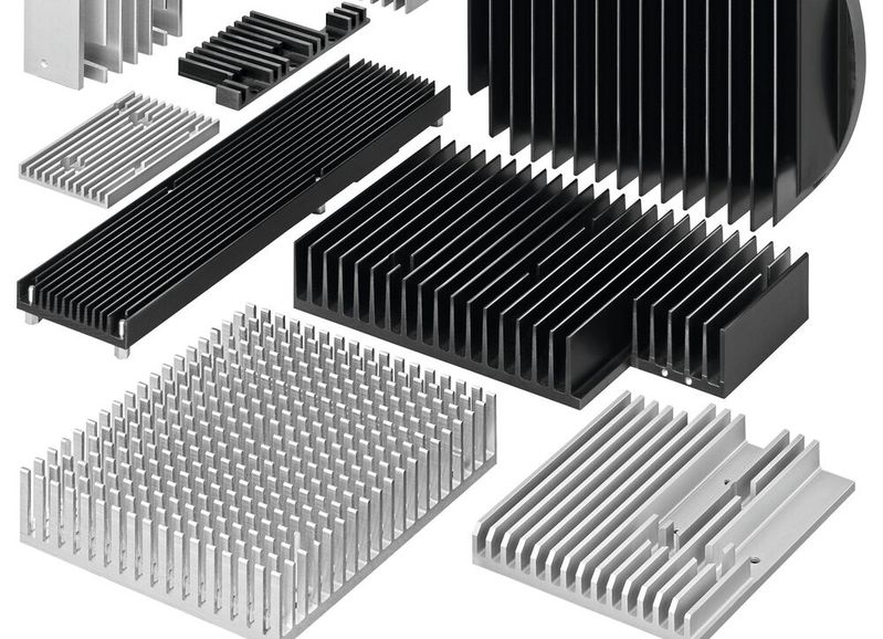
:quality(80)/p7i.vogel.de/wcms/cc/af/ccaf4ad378b1d16f74a1a6d4798d4c02/0132966686v1.jpeg "Thermal management: Custom and mechanically perfectly adapted heat sink solutions for the application provide users with efficient thermal management for many applications.(Image: © Fischer Elektronik)")
:quality(80)/p7i.vogel.de/wcms/8c/a4/8ca4fc587c3c00db245deb159ab109e5/0132966689v1.jpeg "Image 1: High-density heat sinks of the KPK series offer new heat sink designs with a purely mechanical and fully automated pressed fin geometry.(Image: © Fischer Elektronik)")
:quality(80)/p7i.vogel.de/wcms/ce/80/ce801979d4e3c6dc947e277f4bf05630/0132966692v1.jpeg "Image 2: Finned heat sinks of the KGR series are made from a single piece and have no additional thermal resistance from the semiconductor mounting surface to the fin structure.(Image: © Fischer Elektronik)")
:quality(80)/p7i.vogel.de/wcms/19/f7/19f77938e0dcc658e75455cac0073982/0132966696v1.jpeg "Image 3: Skived heat sinks of the KSK series deliver optimal performance for active cooling and stand out with an excellent price-performance ratio.(Image: © Fischer Elektronik)")
:quality(80)/p7i.vogel.de/wcms/ca/90/ca90a13919cdade100d393bb3d2f4b3a/0132724138v1.jpeg "Improved cooling concept: Thanks to the cavity microstructure, known as vascular metamaterials, not only are volume and weight reduced, but the cooling capacity is also increased. (Image:Automoteam)")
:quality(80)/p7i.vogel.de/wcms/2d/da/2ddacc61c32608e3404dff7e9b102f7f/0131807833v1.jpeg "UCS housing with heat sink and heat spreader. (Image: Phoenix Contact)")