


:quality(80)/p7i.vogel.de/wcms/4b/7f/4b7feb398114331dff3d8b6c5e8dc06a/0133877511v1.jpeg "Brandt GmbH designs, manufactures, and services molds and tools for plastic injection molding, metal die casting, and the processing of LSR (liquid silicone rubber). (Image:Brandt)")
:quality(80)/p7i.vogel.de/wcms/db/23/db2332f08461bb166442018b9644b613/0133890143v1.jpeg "The International Monetary Fund (IMF) has revised some of its earlier forecasts for global economic growth upward. Germany, for example, is expected to grow more strongly in 2026 than previously thought. But the IMF has also taken a look at how things are shaping up in the rest of the world... (Image: AI-generated)")
:quality(80)/p7i.vogel.de/wcms/3b/53/3b53eec6903a838b98425d19f21d25ee/0132416085v1.jpeg "Complex progressive dies serve as the basis for stamped and formed parts—such as the copper outer conductors for sensor elements shown here. They are equipped with bending and embossing dies manufactured on the Kern Micro HD. (Image:Quittenbaum, LLC)")
:quality(80)/p7i.vogel.de/wcms/14/43/1443db59695f7eed2a338d16d03a6257/26-09-30-st-ber-ab-hunger-games-bild-1v1.jpeg "For “The Hunger Games: On Stage,” drive systems lift and move grandstand sections with a dynamic load of up to 26 metric tons—each section can accommodate up to 112 spectators. (Source: Troubadour at the Canary Wharf Theatre)")
:quality(80)/p7i.vogel.de/wcms/be/66/be661616d5250d4c3814a25688f3904b/0133917202v1.jpeg "Neuron AI combines 3D vision, touch, hearing, proprioception, and language—along with memory—into a Perception-Language-Action (PLA) model. Robots can grasp objects they cannot see. (Image:Neura)")
:quality(80)/p7i.vogel.de/wcms/c7/12/c712b688dba2262fa3906e3a4c1d2f7d/humanoide-robotikv1.jpeg "“Find a job that the humanoid can actually do, and understand your processes”—that’s the advice robotics expert Sebastian Prinz gives companies so they can benefit from the technology in the long term. (Source: Fraunhofer IEM / Janosch Gruschczyk)")
:quality(80)/p7i.vogel.de/wcms/05/bc/05bcc7390d30da9c23a829f7e96247e3/koch-glserdepalettierung-nahrungsmittelv1.jpeg "Opportunities for automation using robots can be found in all areas of manufacturing, such as in the palletizing of products. (Image:Koch Industrial Systems, LLC)")
:quality(80)/p7i.vogel.de/wcms/a8/0d/a80d9eb978dd47dbd8f390181a039bfc/adobestock-2081783940--design-store-stock-adobe-com-ki-generiertv1.jpeg "We’re showcasing five of the latest innovations for virtual commissioning—from AI copilots and smart browser tools to deep PLC integration. (Source: © Design Store – stock.adobe.com_AI-generated)")
:quality(80)/p7i.vogel.de/wcms/96/89/9689197f666e4aa9bc4a1f395c25d3ef/0133739635v1.jpeg "The 2026 Nobel Prize in Medicine laureates: Karl Deisseroth, Peter Hegemann, and Georg Nagel. (Image:Nobel Prize Outreach)")
:quality(80)/p7i.vogel.de/wcms/8a/c8/8ac8eb7fc2b70f4b72771548e2e2e520/epfl-motor-3v1.jpeg "FiberMotor has a diameter of 1 to 3 mm and consists of two concentric hollow fibers. Each fiber is wrapped in tightly insulated copper wire electrodes that are only slightly thicker than a human hair. (Source: EPFL)")
:quality(80)/p7i.vogel.de/wcms/a7/8a/a78a582a42a96aaaff38bd6b8f97a015/vishal-lal-mit-kernuhrv1.jpeg "It's ticking: Researchers have stabilized the first atomic clock. (Source: PTB)")
:quality(80)/p7i.vogel.de/wcms/36/f9/36f96a206fc408c9a632ce849de1f7fa/newsimage428299v1.jpeg "Polystyrene is used in protective packaging for televisions and electronic devices, in decorative moldings and baseboards for interior home construction, and even in Petri dishes. (Source: Hereon/Marcel Schwickerath)")
:quality(80)/p7i.vogel.de/wcms/a5/25/a52522ce39e6d77c2b8d8cde05f49f9f/0133918381v1.jpeg "Even though this depicts a typical used-car scenario, it symbolizes the current state of German automakers, which are being hit hard, above all, by poor business in China. Here’s a look at the individual automakers ... (Image:AI-generated)")
:quality(80)/p7i.vogel.de/wcms/a6/e9/a6e953bb66750460fdad25708cd5e2d6/0133925000v1.jpeg "What you see here in the X-ray image is a lightweight sandwich-structured component that was developed at the Fraunhofer IMWS in Halle an der Saale in collaboration with partners. What makes it special is that it houses both electronic interfaces and the thermal management system for heat dissipation ... (Image:Fraunhofer IMWS)")
:quality(80)/p7i.vogel.de/wcms/31/9f/319f87514d969d78d06cd8020e519d77/0133896768v1.jpeg "With BasqTrain 35, Talgo aims to develop a new generation of high-speed trains. Modular propulsion technology is intended to facilitate their use on various European rail networks. (Image:Talgo)")
:quality(80)/p7i.vogel.de/wcms/c0/3f/c03f30533805b91651a79fa308960759/0133801213v1.jpeg "The downward spiral in sales that Audi is currently experiencing shows no signs of stopping, as the analysis of the third quarter of 2026 shows ... (Image:Audi)")
:quality(80)/p7i.vogel.de/wcms/8a/d1/8ad1fd2d80399dd663a55b44b0953707/0133918510v1.jpeg "Multiple wireless standards on a single platform: Qualcomm's Dragonwing FWA Gen 6 Elite combines 5G Advanced, satellite communications, and Wi-Fi 8 with on-device AI processing for wireless broadband connectivity. (Image:Qualcomm)")
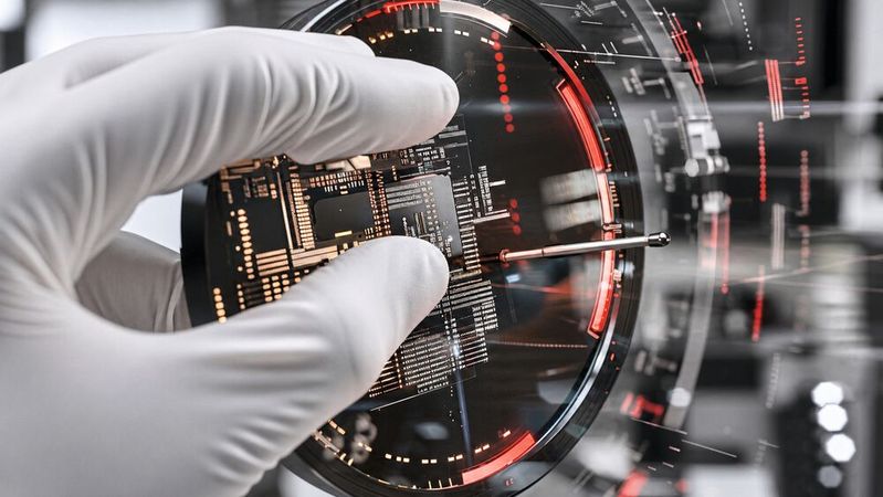
:quality(80)/p7i.vogel.de/wcms/8c/27/8c27323a09724f906aacf549d7cdaf3a/0133923995v1.jpeg "Keysight is working with research institutes to simplify the testing of next-generation semiconductor devices. (Image:Keysight)")
:quality(80)/p7i.vogel.de/wcms/78/92/7892504a95318acd1cd009ce614a33ab/0133939086v1.jpeg "Vishay's nine optical sensors combine an infrared emitter with a PIN photodiode. They enable bidirectional data transmission at speeds of up to 6 Mbit/s, for example in battery management systems for electric vehicles. (Image: Vishay)")
:quality(80)/p7i.vogel.de/wcms/50/81/50811ef8ab18d0626aa6d86dac2c46b4/0133922867v1.jpeg "Encapsulation materials are becoming increasingly important in electronics manufacturing. Particularly in highly integrated chip packages, the requirements for reliability, thermomechanical stability, and processability are rising. (Image:Sumitomo Bakelite)")
Date: 08.12.2025
Naturally, we always handle your personal data responsibly. Any personal data we receive from you is processed in accordance with applicable data protection legislation. For detailed information please see our privacy policy.
Consent to the use of data for promotional purposes
I hereby consent to Vogel Communications Group GmbH & Co. KG, Max-Planck-Str. 7-9, 97082 Würzburg including any affiliated companies according to §§ 15 et seq. AktG (hereafter: Vogel Communications Group) using my e-mail address to send editorial newsletters. A list of all affiliated companies can be found here
Newsletter content may include all products and services of any companies mentioned above, including for example specialist journals and books, events and fairs as well as event-related products and services, print and digital media offers and services such as additional (editorial) newsletters, raffles, lead campaigns, market research both online and offline, specialist webportals and e-learning offers. In case my personal telephone number has also been collected, it may be used for offers of aforementioned products, for services of the companies mentioned above, and market research purposes.
Additionally, my consent also includes the processing of my email address and telephone number for data matching for marketing purposes with select advertising partners such as LinkedIn, Google, and Meta. For this, Vogel Communications Group may transmit said data in hashed form to the advertising partners who then use said data to determine whether I am also a member of the mentioned advertising partner portals. Vogel Communications Group uses this feature for the purposes of re-targeting (up-selling, cross-selling, and customer loyalty), generating so-called look-alike audiences for acquisition of new customers, and as basis for exclusion for on-going advertising campaigns. Further information can be found in section “data matching for marketing purposes”.
In case I access protected data on Internet portals of Vogel Communications Group including any affiliated companies according to §§ 15 et seq. AktG, I need to provide further data in order to register for the access to such content. In return for this free access to editorial content, my data may be used in accordance with this consent for the purposes stated here. This does not apply to data matching for marketing purposes.
Right of revocation
I understand that I can revoke my consent at will. My revocation does not change the lawfulness of data processing that was conducted based on my consent leading up to my revocation. One option to declare my revocation is to use the contact form found at https://contact.vogel.de. In case I no longer wish to receive certain newsletters, I have subscribed to, I can also click on the unsubscribe link included at the end of a newsletter. Further information regarding my right of revocation and the implementation of it as well as the consequences of my revocation can be found in the data protection declaration, section editorial newsletter.
:quality(80)/p7i.vogel.de/wcms/36/ec/36ec46b311c3fb2cf9759ba4843047c5/0129831604v1.jpeg "Keysight and Ericsson enable validation of pre-6G interoperability with real network infrastructure and devices. (Image:Keysight)")
:quality(80)/p7i.vogel.de/wcms/08/ef/08efd9707cae69418f38d5a0a3806657/0128777205v2v1.jpeg "Anritsu and the Finnish research center VTT have achieved a significant breakthrough and validated a complete wireless system in the D-band under realistic conditions for the first time. (Image:Image: Anritsu)")